· AtlasPCB Engineering · Engineering · 11 min read
PCB Bow and Twist: IPC Specification, Measurement Methods & Prevention
Comprehensive guide to PCB bow and twist covering IPC-6012 specifications, TM-650 measurement methods, root causes, prevention strategies, and the impact of warpage on SMT assembly reliability.
Understanding PCB Bow and Twist
Board flatness is one of the most overlooked yet critical quality parameters in PCB manufacturing. As components become smaller, pitches become finer, and reflow processes demand tighter tolerances, even small amounts of warpage can cause catastrophic assembly failures.
Bow and twist are the two primary forms of PCB warpage, and while they’re often discussed together, they describe different deformation modes:
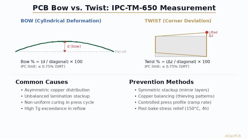
Bow (弓形翘曲)
Bow is a uniform, cylindrical curvature of the board. Imagine holding a PCB by two opposite edges — if it curves uniformly like a section of a cylinder, that’s bow. Key characteristics:
- The curvature is approximately constant along one axis
- When placed on a flat surface, the board contacts along two opposite edges (or the center) with gaps at the other edges (or center)
- Bow is relatively predictable and often caused by asymmetric copper distribution
Twist (扭曲)
Twist is a diagonal warpage where the board deforms in a helical or propeller-like fashion. The defining test:
- Hold three corners of the board flat against a reference surface
- If the fourth corner lifts off the surface, the board has twist
- Twist creates a more complex deformation pattern than bow
In practice, most warped PCBs exhibit a combination of bow and twist, making flatness control a multi-dimensional challenge.
IPC Specifications for Bow and Twist
IPC-6012: Qualification and Performance Specification
IPC-6012 defines the maximum acceptable bow and twist as a percentage of the board diagonal:
| Assembly Type | Maximum Bow & Twist | Application |
|---|---|---|
| Surface mount (SMT) | 0.75% | Any board with SMT components |
| Through-hole only | 1.5% | Boards with only through-hole components |
| BGA / Fine-pitch | 0.5% (recommended) | Critical applications with <0.5 mm pitch |
Calculation formula:
Warpage % = (Maximum Deviation ÷ Diagonal Length) × 100
Example calculations:
For a board measuring 100 × 160 mm:
- Diagonal = √(100² + 160²) = 188.7 mm
- SMT limit (0.75%): Maximum deviation = 188.7 × 0.0075 = 1.42 mm
- THT limit (1.5%): Maximum deviation = 188.7 × 0.015 = 2.83 mm
For a board measuring 200 × 250 mm:
- Diagonal = √(200² + 250²) = 320.2 mm
- SMT limit (0.75%): Maximum deviation = 320.2 × 0.0075 = 2.40 mm
IPC Class-Specific Considerations
While the 0.75%/1.5% limits apply across IPC classes, the practical implications vary:
- IPC Class 1 (General Electronics): 0.75% for SMT, 1.5% for THT. Standard acceptance testing.
- IPC Class 2 (Dedicated Service Electronics): Same percentages, but tighter process controls expected. See our [DFM checklist]/blog/pcb-dfm-checklist/) for Class 2 recommendations.
- IPC Class 3 (High Performance Electronics): 0.75% for SMT, but customers often specify tighter limits (0.5% or 0.3%) for critical applications. Refer to our [IPC Class 3 requirements guide]/blog/ipc-class-3-requirements/) for comprehensive Class 3 specifications.
JEDEC and Other Standards
Beyond IPC-6012, other standards address PCB flatness:
- JEDEC J-STD-020: Defines moisture sensitivity and reflow conditions — boards must maintain flatness throughout reflow thermal profiles
- IPC-A-610: Acceptability standard for assembled boards — references IPC-6012 limits for incoming board inspection
- IPC-SM-782: Surface mount land pattern standard — assumes boards meet flatness requirements
Measurement Methods
IPC-TM-650 Method 2.4.22
The official IPC test method for bow and twist measurement:
Equipment required:
- Granite surface plate (Grade A or B, flatness ≤0.005 mm per 300 mm)
- Feeler gauges or precision height gauge
- Measurement resolution: 0.05 mm minimum
Procedure:
- Conditioning: Store the board at 23°C ± 2°C, 50% ± 5% RH for minimum 4 hours
- Placement: Place the board convex-side-up on the surface plate
- Measurement: Measure the maximum gap between the board and the surface plate
- Bow measurement: Determine the maximum deviation along each principal axis of the board
- Twist measurement: Hold three corners in contact with the surface plate and measure the lift of the fourth corner
- Calculation: Express the result as a percentage of the diagonal length
For bow:
- Place the board on the flat surface
- Measure the maximum gap at the center (for a concave board) or at the edges (for a convex board)
- Report the maximum value
For twist:
- Measure the diagonal deviation
- The twist value is the distance the fourth corner lifts from the reference plane
Automated Measurement Systems
Modern fabrication facilities use automated measurement equipment:
Shadow Moiré / Phase-Shift Moiré:
- Non-contact optical measurement
- Creates a 3D surface map of the board
- Can measure bow, twist, and localized warpage simultaneously
- Resolution: typically 5–10 µm
- Measures room-temperature flatness
Laser Profilometry:
- Point or line laser scans across the board surface
- Generates a height map with sub-micron resolution
- Fast measurement (seconds per board)
- Suitable for in-line production inspection
Thermal Warpage Measurement (Shadow Moiré at Temperature):
- Measures warpage at elevated temperatures (up to 260°C+)
- Critical for understanding warpage behavior during reflow
- Board may be flat at room temperature but warp significantly at reflow temperature
- Equipment: Akrometrix TherMoiré or equivalent
When to Measure
- After panel fabrication: Before singulation, to verify process control
- After singulation: Individual boards, the official inspection point per IPC-6012
- After baking: If boards have been stored and may have absorbed moisture
- During reflow simulation: For critical applications, measure warpage at temperature
Root Causes of PCB Warpage
Copper Balance (Most Common Cause)
Uneven copper distribution between the top and bottom halves of the stackup is the primary cause of bow:
How it works:
- Copper has a lower CTE than FR-4 (17 ppm/°C vs ~14-18 ppm/°C in XY, but ~60-70 ppm/°C in Z)
- A layer with more copper restrains expansion more than a layer with less copper
- During thermal cycling (lamination, reflow), the asymmetric constraint creates bending moments
- The board bows toward the side with more copper (the more-constrained side)
Design solutions:
- Balance copper percentages between symmetric layer pairs (L1 vs. Ln, L2 vs. Ln-1, etc.)
- Target copper balance within ±10% between paired layers
- Add copper thieving (non-functional copper fill) to balance sparse layers
- Use our [stackup calculator]/blog/pcb-stackup-calculator/) to plan balanced configurations
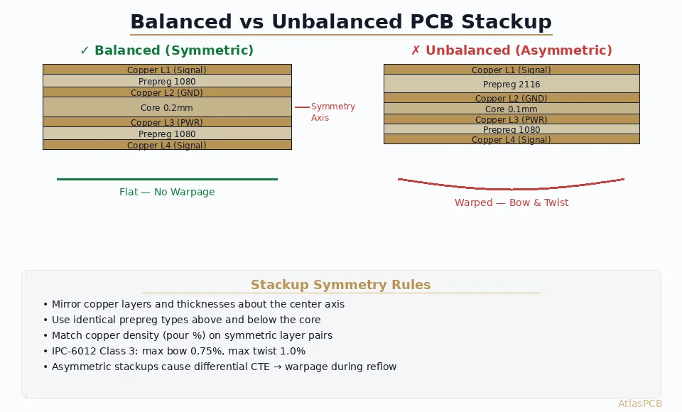
Stackup Asymmetry
Beyond copper, the laminate materials themselves must be symmetric:
- Core/prepreg arrangement: Use identical materials in mirror-symmetric positions
- Glass style: The same glass weave should be used for corresponding prepreg layers
- Resin content: Matched resin content ensures symmetric CTE behavior
- Thickness: Symmetric thickness distribution around the board centerline
Example of a balanced 6-layer stackup:
L1 (Signal) — Target 40% copper
  Prepreg 1080 (65% RC)
L2 (Ground) — Target 80% copper
  Core 0.2mm
L3 (Signal) — Target 35% copper
  ← CENTERLINE →
L4 (Signal) — Target 35% copper
  Core 0.2mm
L5 (Power) — Target 80% copper
  Prepreg 1080 (65% RC)
L6 (Signal) — Target 40% copper
Lamination Process Parameters
Improper lamination directly causes warpage:
- Temperature: Non-uniform heating across the panel causes differential curing
- Pressure: Insufficient or uneven pressure allows resin flow to redistribute asymmetrically
- Cool-down rate: Rapid cooling creates thermal stress gradients — controlled cool-down (<3°C/min from Tg) reduces warpage
- Book construction: The arrangement of panels in the lamination press affects pressure distribution
Reflow-Induced Warpage
PCBs can be flat at room temperature but warp significantly during reflow:
The “smile” and “frown” effect:
- During ramp-up (below Tg): Board may bow in one direction as CTE differences create stress
- Near Tg transition: Glass transition softens the resin, releasing some stress but allowing new deformation
- Above Tg: Dramatically increased Z-axis CTE causes complex warpage behavior
- During cooling: The board may not return to its pre-reflow shape if stress exceeds the elastic limit
For multilayer boards, this dynamic warpage during reflow is often the most critical issue. See our [warpage control guide]/blog/pcb-warpage-control-multilayer/) for advanced mitigation strategies.
Material-Related Causes
- Moisture absorption: FR-4 absorbs 0.1–0.3% moisture by weight, causing swelling. Asymmetric moisture content (e.g., one side exposed to humidity) creates warpage
- Resin system: Higher-Tg resins generally produce more warpage due to greater CTE mismatch above Tg
- Filler content: Filled resin systems (e.g., with silica filler) have lower CTE and better dimensional stability
- Glass weave: Different glass styles have different CTE characteristics — mismatched styles between layers contribute to warpage
Processing-Related Causes
- Uneven plating: Copper electroplating adds significant stress. If plating thickness varies across the board, it creates asymmetric stress. Refer to our [copper weight guide]/blog/pcb-copper-weight-thickness/) for plating thickness considerations.
- Solder mask curing: The solder mask is a polymer that shrinks during curing. If the cure profile is uneven (top vs. bottom), it adds bow.
- Routing stress: Board singulation (routing or V-scoring) releases stress from the panel, potentially changing flatness.
- Solder mask type: Different solder mask formulations have different shrinkage characteristics — liquid photoimageable (LPI) vs. dry film solder mask.
Prevention Strategies
Design Phase
Balance your copper distribution
- Run copper balance analysis in your CAD tool
- Add copper thieving to sparse layers (hatched or solid fill in non-critical areas)
- Keep copper percentage within ±10% between paired layers
Design a symmetric stackup
- Mirror material types and thicknesses around the centerline
- Avoid mixing different core/prepreg materials asymmetrically
- Specify glass style and resin content in your fabrication notes
Consider board aspect ratio
- Long, narrow boards are more susceptible to bow than square boards
- If possible, keep the board aspect ratio (length/width) below 3:1
- Add stiffening features (rails, tooling holes) to large, thin boards
Manage thermal mass distribution
- Large copper fills (ground/power planes) should be balanced
- Heavy components with large thermal pads add localized mass — distribute them when possible
Fabrication Phase
Specify warpage limits in fabrication notes
- State the IPC class and maximum bow/twist percentage
- For critical designs, specify tighter-than-IPC limits
- Include measurement method reference (IPC-TM-650 2.4.22)
Control lamination parameters
- Work with your fabricator to ensure proper lamination profiles
- Request controlled cool-down rates for warpage-sensitive designs
- Consider post-lamination stress relief baking (150°C, 2–4 hours)
Pre-bake before reflow
- Bake boards at 120°C for 2–4 hours (or per IPC-1601) before assembly to remove moisture
- This is especially important for boards stored more than 24 hours after unpacking
Assembly Phase
Optimize reflow profile
- Minimize time above liquidus (TAL) to reduce thermal stress
- Use controlled cool-down rates (<3°C/sec recommended)
- Consider using support fixtures for thin or large boards during reflow
Use board support in the reflow oven
- Center-board support pins prevent sagging in long ovens
- Edge rails with board guides maintain alignment
- Custom fixtures for critical assemblies
Monitor and feedback
- Measure incoming board warpage before assembly
- Track rejects by warpage cause to feed back to board fabrication
- Establish incoming inspection criteria tied to your assembly capabilities
Impact of Warpage on Assembly
SMT Component Placement
| Warpage Level | 0201/01005 | 0402 | 0805+ | QFP | BGA |
|---|---|---|---|---|---|
| <0.5% | OK | OK | OK | OK | OK |
| 0.5–0.75% | Marginal | OK | OK | OK | Marginal |
| 0.75–1.0% | Fail | Marginal | OK | Marginal | Fail |
| >1.0% | Fail | Fail | Marginal | Fail | Fail |
BGA is the most warpage-sensitive component due to its area-array solder joint geometry. A warped board under a BGA creates:
- Open joints at the corners (concave warpage) or center (convex warpage)
- Head-in-pillow defects (solder ball contacts paste but doesn’t fully coalesce)
- Non-wet opens that may pass initial testing but fail in thermal cycling
Specific Failure Modes
Tombstoning (chip components):
- Unequal paste contact due to local warpage lifts one end of the component during reflow
- More common with 0201 and smaller components
- Particularly problematic when warpage combines with paste printing variation
BGA opens:
- The most costly warpage-related defect
- Can be hidden (no visual indication) and requires X-ray inspection
- May only appear at specific BGA locations (corners or center, depending on warpage direction)
Solder bridging:
- Warpage can change the stencil-to-board gap during paste printing
- Excess paste in low areas bridges between fine-pitch leads
- Most common with QFP and fine-pitch connectors
For more on how warpage affects thermal performance, see our [thermal management guide]/blog/pcb-thermal-management/).
Dynamic Warpage: The Reflow Challenge
Understanding Dynamic Warpage
Static (room-temperature) warpage is what IPC-6012 measures, but dynamic warpage — the deformation that occurs during the reflow thermal cycle — is often more important for assembly yield.
A board that measures 0.3% warpage at room temperature might reach 1.5% at peak reflow temperature, then settle to 0.5% after cooling. The maximum warpage at any point during reflow determines assembly success or failure.
Dynamic Warpage Measurement
Shadow Moiré at temperature (e.g., Akrometrix TherMoiré) profiles the board’s warpage throughout the reflow cycle:
Typical dynamic warpage profile for a multilayer board:
- 25°C to 150°C: Gradual increase in warpage as CTE mismatch builds stress
- 150°C to 217°C (pre-reflow): May see a warpage direction change near Tg
- 217°C to 245°C (reflow zone): Maximum warpage typically occurs here — the resin is above Tg and solder is molten
- 245°C to 217°C (solidification): Warpage direction may reverse
- Cooling to 25°C: Final warpage — may be different from initial warpage
Critical threshold: The warpage at the moment of solder solidification (~217°C for SAC305) determines the final joint geometry.
Design for Dynamic Warpage
To minimize dynamic warpage:
- Use lower-CTE materials (filled resin systems, low-Dk laminates with silica filler)
- Increase board thickness (stiffer boards resist deformation)
- Reduce total thermal excursion (lower peak reflow temperature with appropriate solder paste)
- Balance copper at all temperatures (the balance that works at room temperature must also work above Tg)
Special Considerations
Thin Boards (<0.8 mm)
Thin boards are inherently more flexible and susceptible to warpage:
- Apply tighter copper balance tolerances (±5% between paired layers)
- Consider using stiffeners (FR-4 or metal) in non-critical areas
- Specify a tighter warpage limit (0.5% or lower)
- Always use reflow support fixtures during assembly
Large Boards (>300 mm diagonal)
Large boards amplify the absolute warpage for a given percentage:
- A 500 mm diagonal board at 0.75% warpage = 3.75 mm deviation — enough to cause severe assembly issues
- Consider sub-paneling (keeping individual boards small and arraying them)
- Use mechanical stiffening features (tooling rails, panel borders)
Lead-Free Reflow Considerations
Lead-free solder (SAC305) requires higher reflow temperatures (~245°C peak vs. ~225°C for SnPb):
- Higher temperature means more thermal stress and greater warpage
- Boards must maintain flatness at higher temperatures
- Consider mixed-alloy approaches (SnBiAg for temperature-sensitive areas) where applicable
Conclusion
PCB bow and twist, while seemingly a simple dimensional parameter, impacts virtually every aspect of electronics manufacturing from paste printing through final test. The key points:
- IPC-6012 limits: 0.75% for SMT, 1.5% for THT — express as percentage of diagonal length
- Copper balance is the single most effective design-stage mitigation — target ±10% or better between paired layers
- Symmetric stackup construction (materials, thicknesses, glass styles) is essential
- Dynamic warpage during reflow is often more critical than static room-temperature flatness
- Thin boards and large boards require special attention and tighter specifications
- Pre-baking and controlled reflow profiles are essential process controls
Early collaboration between design, fabrication, and assembly teams is the most effective way to prevent warpage issues. Atlas PCB offers comprehensive warpage analysis and prevention support from design through production.
Atlas PCB specializes in warpage-controlled PCB fabrication with advanced lamination processes, symmetric stackup design, and comprehensive flatness testing. Contact us for engineering support and a free DFM review on your next project.
Further Reading
- [PCB Rigid-Flex Bend Zone Reliability: Design Rules, Material Selection & Lifecycle Testing]/blog/pcb-rigid-flex-bend-zone-reliability/)
- [ENEPIG vs ENIG Surface Finish: Complete Comparison for Wire Bonding, Solderability, and Long-Term Reliability]/blog/enepig-vs-enig-surface-finish-wire-bonding/)
- [PCB Surface Finish Comparison: OSP vs HASL vs Immersion Silver vs ENIG for Assembly Reliability]/blog/pcb-surface-finish-osp-hasl-enig-immersion-silver-comparison/)
- [PCB Electrical Testing: Flying Probe vs Bed-of-Nails Fixture Testing Compared]/blog/pcb-electrical-testing-flying-probe-vs-fixture/)
- [Medical PCB Manufacturing: FDA Compliance, Traceability & Reliability]/blog/medical-pcb-manufacturing-requirements/)
- Our Manufacturing Capabilities
About AtlasPCB — We specialize in complex PCB manufacturing for HDI, RF, and high-reliability applications. Explore our PCB assembly services, or get an full PCB manufacturing capabilities . Every order includes free engineering review. Get your quote.
Reviewed by AtlasPCB Engineering Team — IPC-certified manufacturing specialists with 15+ years of production experience in HDI, RF, and high-reliability PCB fabrication. Content based on factory floor data and real customer design reviews.
- bow-twist
- warpage
- ipc-6012
- flatness
- reflow