· AtlasPCB Engineering · Engineering · 9 min read
AI Hardware PCB Thermal Management: Advanced Multilayer Stackup Design for 1000W+ Processing Units
Master thermal management in multilayer PCBs for AI hardware. Learn advanced stackup techniques, copper balancing, and thermal via design for 1000W+ GPU/TPU applications with proper heat dissipation.
Introduction: The Thermal Challenge in AI Hardware
Modern AI accelerators have pushed power consumption to unprecedented levels. NVIDIA’s H200 GPU consumes 700W, while next-generation AI training chips are targeting 1000W+ in packages smaller than a credit card. This power density—equivalent to a stovetop burner compressed into a few square centimeters—creates thermal management challenges that fundamentally reshape PCB design.
Traditional multilayer PCB thermal management techniques, adequate for 50-200W processors, fail catastrophically at AI hardware power levels. Junction temperatures exceeding 105°C trigger thermal throttling, reducing AI training performance by 20-40%. Worse, thermal cycling stress can cause solder joint fatigue and via barrel cracking, leading to expensive field failures.
This guide explores advanced thermal management strategies for multilayer PCBs supporting 1000W+ AI processors, covering stackup architecture, copper distribution, thermal via design, and validation techniques that keep AI hardware running at peak performance.
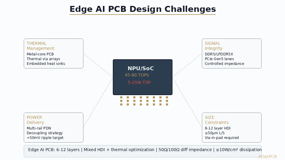
Understanding AI Hardware Thermal Challenges
Power Density Evolution
The progression in AI chip power density illustrates the magnitude of thermal challenges:
Historical progression:
- 2020: GPU ~250W in 750 mm² package (0.33 W/mm²)
- 2024: H100 GPU ~700W in 814 mm² package (0.86 W/mm²)
- 2026: Next-gen AI chips ~1200W in 900 mm² package (1.33 W/mm²)
For comparison, typical CPU power densities remain at 0.1-0.3 W/mm², making AI hardware 3-4× more thermally challenging.
Heat Generation Patterns
Unlike uniform CPU heat generation, AI accelerators create highly localized hotspots:
- Compute units: 70-80% of total power in small die areas
- Memory interfaces: High-speed I/O generating 15-20% of power
- Power delivery: On-die regulators contributing 5-10%
- Temporal variations: Training workloads create dynamic power spikes
Thermal Management Objectives
Effective AI hardware PCB thermal design must achieve:
- Junction temperature: <85°C under full load (vs. 105°C thermal limit)
- Thermal cycling: <50°C delta-T to minimize solder fatigue
- Gradient management: <10°C/mm to prevent die stress
- Transient response: <2°C overshoot during power spikes
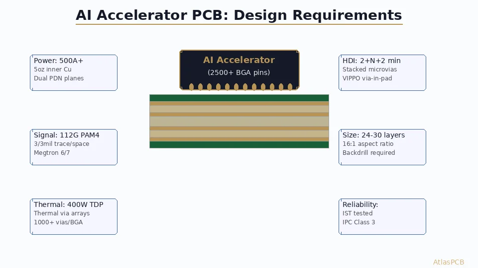
Advanced Multilayer Stackup Architecture
Layer Count Optimization
AI hardware PCBs typically require 16-32 layers to manage both thermal and electrical requirements:
Typical 20-layer AI PCB stackup:
- L1: Component placement (2 oz copper)
- L2: Ground plane (2 oz copper, thermal vias)
- L3: High-speed signals (0.5 oz copper)
- L4: Power plane - 12V (2 oz copper)
- L5: Signal routing (0.5 oz copper)
- L6: Ground plane (1 oz copper)
- L7: Signal routing (0.5 oz copper)
- L8: Power plane - 3.3V (1 oz copper)
- L9: Signal routing (0.5 oz copper)
- L10: Ground plane (2 oz copper, thermal vias)
- L11: Signal routing (0.5 oz copper)
- L12: Power plane - 1.8V (1 oz copper)
- L13: Signal routing (0.5 oz copper)
- L14: Ground plane (1 oz copper)
- L15: Signal routing (0.5 oz copper)
- L16: Power plane - 1.2V (2 oz copper)
- L17: Signal routing (0.5 oz copper)
- L18: Ground plane (2 oz copper, thermal vias)
- L19: Signal routing (0.5 oz copper)
- L20: Component placement (2 oz copper)
Thermal Plane Distribution Strategy
Copper weight selection balances thermal performance with manufacturing constraints:
- Thermal planes: 2-4 oz copper for maximum heat spreading
- Signal layers: 0.5-1 oz copper to minimize dielectric thickness
- Power planes: 1-2 oz copper based on current density requirements
- Outer layers: 2 oz copper for heat sink interface
Dielectric Selection for Thermal Performance
High thermal conductivity dielectrics improve through-plane heat transfer:
Standard FR-4: 0.3 W/m·K thermal conductivity High-Tg FR-4: 0.4 W/m·K (improved filler content)
Bergquist Tg-Flex: 1.0 W/m·K (thermally enhanced) Rogers RO4450T: 0.80 W/m·K (specialized thermal laminate)
For critical thermal paths under AI processors, high-conductivity prepregs justify the 2-3× cost premium.
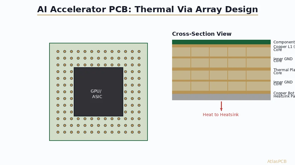
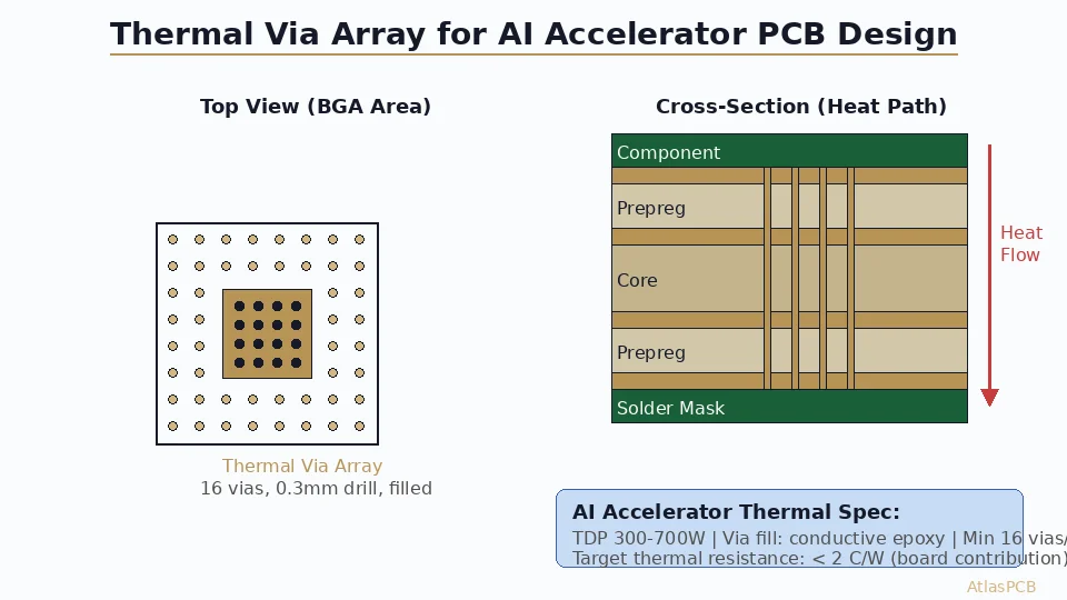
Thermal Via Design and Implementation
Thermal Via Array Architecture
Thermal vias provide the primary path for heat transfer from component to heat sink. Unlike electrical vias, thermal via design prioritizes heat conduction over signal integrity:
Standard thermal via specifications:
- Via diameter: 0.2-0.3 mm (8-12 mil)
- Via pitch: 0.5-0.8 mm center-to-center
- Copper fill: Recommended for improved conductivity
- Via density: 40-60% fill factor in thermal zones
Via-in-Pad Implementation
For BGA packages with fine pitch (0.4-0.5 mm), [via-in-pad design]/blog/via-in-pad-design/) becomes essential:
Design considerations:
- Via size: Maximum 0.1 mm smaller than pad diameter
- Copper fill: Required for planar solder joint formation
- Cap plating: Additional copper over filled vias
- Solder mask: Via plugging to prevent solder wicking
Thermal Via Fill Technology
Via fill methods impact thermal performance:
Copper fill:
- Thermal conductivity: ~400 W/m·K
- Process: Electroplating or paste fill
- Advantage: Maximum conductivity
- Challenge: Process complexity, cost
Conductive paste fill:
- Thermal conductivity: 5-20 W/m·K
- Process: Screen printing, curing
- Advantage: Lower cost, simpler process
- Application: Non-critical thermal paths
No fill (air gap):
- Thermal conductivity: ~0.025 W/m·K
- Advantage: Standard process, lowest cost
- Application: Electrical vias only
Copper Distribution and Heat Spreading
Copper Balancing for Thermal Performance
Copper balance affects both thermal performance and manufacturing yield:
Thermal optimization approach:
- Under processor: Maximum copper pour (80-90% fill)
- Thermal paths: Continuous copper planes connecting vias
- Signal areas: Reduced copper to maintain impedance
- Manufacturing balance: Minimum 20% copper per layer overall
Power Plane Design for Heat Spreading
Power planes serve dual roles as current distribution and thermal spreading:
12V plane design (highest power):
- Copper weight: 2-4 oz for current/thermal capacity
- Via connections: Multiple connections to thermal vias
- Plane splits: Minimize to maintain thermal continuity
- Thermal relief: Avoided in high-power sections
Low-voltage planes (1.0-1.8V):
- Current density: Higher current, requires adequate copper
- Thermal contribution: Significant due to high current flow
- Decoupling integration: Embedded capacitance where possible
- Via transitions: Thermal vias can double as power connections
Ground Plane Thermal Integration
Ground planes provide excellent thermal spreading when properly designed:
Solid ground approach:
- Thermal continuity: Uninterrupted heat paths
- Via integration: Direct thermal via connection
- Signal compatibility: Maintains signal integrity
- EMI benefits: Enhanced shielding effectiveness
Split ground challenges:
- Thermal barriers: Slots interrupt heat paths
- Via isolation: Thermal vias may lose ground connection
- Design complexity: Routing around thermal requirements
Advanced Thermal Management Techniques
Embedded Cooling Channels
Microchannel cooling integrates directly into PCB construction:
Channel specifications:
- Channel width: 0.5-2.0 mm
- Channel depth: 0.2-0.5 mm (within dielectric)
- Coolant: Dielectric fluids, water-glycol mixtures
- Flow rates: 50-200 ml/min per channel
Manufacturing approach:
- Laser ablation: Precise channel formation
- Lamination sealing: Specialized prepreg bonding
- Manifold integration: External connections to cooling system
- Leak testing: Critical quality control step
Phase Change Material (PCM) Integration
PCM layers provide thermal buffering for transient loads:
Material selection:
- Melting point: 60-80°C (below component limits)
- Thermal capacity: 150-250 J/g latent heat
- Thickness: 0.1-0.5 mm embedded layers
- Location: Between thermal planes near processors
Thermal Interface Material (TIM) Optimization
TIM selection critically impacts heat transfer to heat sinks:
High-performance options:
- Thermal grease: 3-8 W/m·K, lowest cost
- Thermal pads: 1-15 W/m·K, consistent thickness
- Liquid metal: 70+ W/m·K, maximum performance
- Phase change TIM: 3-5 W/m·K, gap filling
Simulation and Thermal Analysis
Finite Element Analysis (FEA)
Thermal simulation validates designs before prototyping:
Analysis parameters:
- Power mapping: Accurate component power distribution
- Material properties: Temperature-dependent conductivity
- Boundary conditions: Heat sink, ambient cooling
- Transient analysis: Dynamic power profile effects
Key simulation tools:
- Ansys Icepak: Comprehensive electronics cooling
- FloTHERM: Specialized PCB thermal analysis
- COMSOL: General-purpose multiphysics simulation
- Altium Designer: Integrated thermal analysis capability
Validation Methodologies
Thermal measurement techniques:
Thermocouple arrays:
- Placement: Strategic locations across PCB
- Accuracy: ±0.5°C with proper calibration
- Response time: Suitable for steady-state analysis
- Limitations: Point measurements, limited spatial resolution
Infrared thermography:
- Coverage: Full PCB surface mapping
- Resolution: 0.1°C temperature, 100 μm spatial
- Real-time: Dynamic thermal behavior observation
- Limitations: Surface temperature only, emissivity correction
Thermal test vehicles:
- Power resistors: Controlled heat source simulation
- Thermal via effectiveness: Direct via performance measurement
- Material validation: Actual vs. specified properties
- Process verification: Manufacturing variation assessment
Design for Manufacturing (DFM) Considerations
Via Formation Challenges
Thermal via arrays create unique manufacturing challenges:
Drilling considerations:
- Tool wear: High via density accelerates drill wear
- Registration: Maintaining via position accuracy
- Smear removal: Critical for via electrical continuity
- Aspect ratio: Depth-to-diameter limits for reliability
Plating uniformity:
- Current distribution: Dense via arrays affect plating
- Thickness variation: Center vs. edge via differences
- Fill quality: Void-free copper fill requirements
- Process control: Statistical monitoring of via quality
Copper Weight Manufacturing Limits
Heavy copper processing has practical constraints:
Standard capabilities:
- 2 oz copper: Standard process, high yield
- 4 oz copper: Achievable with yield impact
- 6+ oz copper: Specialized process, limited suppliers
- Line width: Minimum features scale with copper weight
Design implications:
- Etching compensation: Heavier copper requires wider initial traces
- Registration tolerance: Thicker copper affects layer-to-layer alignment
- Via formation: Heavier copper increases drilling difficulty
- Cost impact: Exponential increase beyond 2 oz copper
Quality Control Requirements
Thermal performance validation:
Cross-sectioning analysis:
- Via fill quality: Void content, copper continuity
- Layer adhesion: Delamination risk assessment
- Copper thickness: Actual vs. specified measurements
- Thermal via connectivity: Electrical continuity verification
Thermal cycling testing:
- Test conditions: -40°C to +125°C, 1000+ cycles
- Failure criteria: Resistance change, visual inspection
- Sample size: Statistical confidence requirements
- Accelerated testing: Elevated temperature/humidity stress
Cost Optimization Strategies
Selective Thermal Enhancement
Targeted thermal design optimizes cost-performance balance:
High-performance zones:
- Under processor: Maximum thermal via density, heavy copper
- Critical paths: Enhanced materials, optimized routing
- Heat sink interface: Premium thermal interface materials
Standard zones:
- Low-power areas: Standard thermal management techniques
- Signal routing: Conventional stackup, standard materials
- I/O sections: Cost-effective thermal solutions adequate
Alternative Material Strategies
Cost-effective thermal improvements:
Hybrid constructions:
- Critical layers: High thermal conductivity dielectrics
- Non-critical layers: Standard FR-4 materials
- Transition management: Careful CTE matching between materials
- Manufacturing complexity: Process compatibility considerations
Copper pour optimization:
- Smart copper distribution: Maximum thermal benefit per copper ounce
- Via sharing: Electrical and thermal via consolidation
- Plane partitioning: Separate thermal and electrical requirements
- Manufacturing balance: Adequate copper balance for yield
Industry Trends and Future Developments
Next-Generation Cooling Technologies
Emerging thermal management approaches:
3D vapor chambers:
- Integration: Embedded vapor chambers in PCB substrates
- Performance: 10-50× thermal conductivity improvement
- Manufacturing: Specialized lamination and sealing processes
- Applications: Ultra-high-power AI accelerators (1500W+)
Liquid cooling integration:
- Direct die cooling: Coolant circulation through PCB channels
- Dielectric coolants: Direct component immersion cooling
- Pumping systems: Micro-pumps integrated with PCB assembly
- Reliability: Long-term leak prevention and maintenance
Advanced Materials Development
Next-generation thermal materials:
Graphene-enhanced dielectrics:
- Thermal conductivity: 5-10× improvement over standard FR-4
- Electrical properties: Maintained dielectric performance
- Cost trajectory: Decreasing toward practical implementation
- Availability: Limited production, specialty applications
Carbon nanotube composites:
- Anisotropic conductivity: Directional thermal enhancement
- Mechanical properties: Improved strength and reliability
- Processing challenges: Dispersion and orientation control
- Applications: Specialized high-performance applications
Conclusion: Mastering AI Hardware Thermal Design
Successfully managing thermal challenges in 1000W+ AI hardware requires a fundamental shift from traditional PCB thermal management approaches. The combination of extreme power densities, localized hotspots, and performance requirements demands advanced techniques across every aspect of multilayer PCB design.
Key success factors include:
- Systematic thermal planning: Thermal considerations must drive stackup architecture from concept phase
- Advanced via technology: Dense thermal via arrays with proper fill technology
- Material selection: Strategic use of high-performance thermal materials where justified
- Simulation validation: Comprehensive thermal modeling before prototyping
- Manufacturing partnership: Close collaboration with suppliers capable of thermal-optimized processes
The cost-performance optimization requires careful balance between thermal enhancement and manufacturing practicality. Not every layer needs premium materials, and not every via needs copper fill—but identifying where these technologies provide maximum benefit is critical.
As AI hardware continues pushing power boundaries toward 2000W and beyond, today’s advanced thermal management techniques will become tomorrow’s minimum requirements. Organizations that master these techniques now will be positioned to succeed in the increasingly thermal-constrained AI hardware landscape.
Future-proofing strategies should include:
- Scalable thermal architectures that can adapt to higher power levels
- Manufacturing process development for next-generation thermal technologies
- Thermal validation capabilities matching the pace of AI hardware evolution
- Supply chain partnerships with advanced thermal management expertise
Designing thermal management for next-generation AI hardware? Our engineering team specializes in [multilayer PCB thermal design]/blog/pcb-thermal-via-design-en/) and [high-power applications]/blog/heavy-copper-pcb/). Contact us to discuss your thermal management challenges and manufacturing capabilities for AI hardware applications.
Further Reading
- [Aluminum PCB Thermal Design for High-Power LED and Motor Drivers: Material Selection, Stackup, and DFM Guide]/blog/aluminum-pcb-thermal-design-led-motor-driver/)
- [PCB Design for GaN and SiC Power Devices: Thermal Management, Layout Rules, and Material Selection]/blog/pcb-design-gan-sic-power-devices-thermal-layout/)
- [High Layer Count PCB Challenges: Designing and Manufacturing 20 to 68 Layer Boards]/blog/high-layer-count-pcb-challenges/)
- [PCB Thermal Management: Heat Dissipation Techniques for Reliable Electronics]/blog/pcb-thermal-management/)
- [Aluminum PCB for LED Applications: Design, Benefits, and Best Practices]/blog/aluminum-pcb-led-applications/)
- Rigid PCB Manufacturing
About AtlasPCB — We specialize in complex PCB manufacturing for HDI, RF, and high-reliability applications. Explore our multilayer PCB fabrication up to 30 layers, or get an aluminum and metal-core PCB services . Every order includes free engineering review. Get your quote.
Reviewed by AtlasPCB Engineering Team — IPC-certified manufacturing specialists with 15+ years of production experience in HDI, RF, and high-reliability PCB fabrication. Content based on factory floor data and real customer design reviews.
- multilayer PCB
- thermal management
- AI hardware
- thermal vias
- copper balancing
- high power PCB