· AtlasPCB Engineering · Engineering · 8 min read
Reinforcement Learning PCB Layout: How Quilter's AI Engine Solves Constraint-Aware Board Generation
Technical deep-dive into reinforcement learning approaches for autonomous PCB layout. Examines Quilter's physics-driven AI engine, constraint compilation, DRC-clean generation, and the implications for hardware design workflows in 2026 and beyond.
The Shift from Autorouting to Autonomous Layout
PCB layout automation has been a goal of the EDA industry for over four decades. From the earliest maze routers of the 1980s to the topological routers of the 2000s, every generation promised to eliminate the manual layout bottleneck. Every generation fell short.
The fundamental problem: PCB layout is not just a routing problem. It’s a multi-objective optimization across electrical performance, thermal management, mechanical constraints, manufacturing yield, signal integrity, and EMI compliance — all simultaneously. Traditional algorithms excel at one dimension (shortest path, fewest vias) but fail catastrophically when asked to balance competing objectives the way an experienced layout engineer intuitively does.
Reinforcement learning changes the equation. Instead of programming rules about what makes a good layout, RL trains an agent by having it generate millions of layouts and evaluating the outcomes. The agent develops policies — learned behaviors — that encode complex trade-offs no human programmer could explicitly specify.
In 2026, this approach has moved from research papers to production tools. Quilter has demonstrated autonomous layout of a complete single-board computer (their “Project Speedrun”) from schematic to fabrication-ready Gerber files, validated through power-on testing under real workloads. This represents a qualitative shift from “AI-assisted” to “AI-driven” PCB design.

How Reinforcement Learning PCB Layout Works
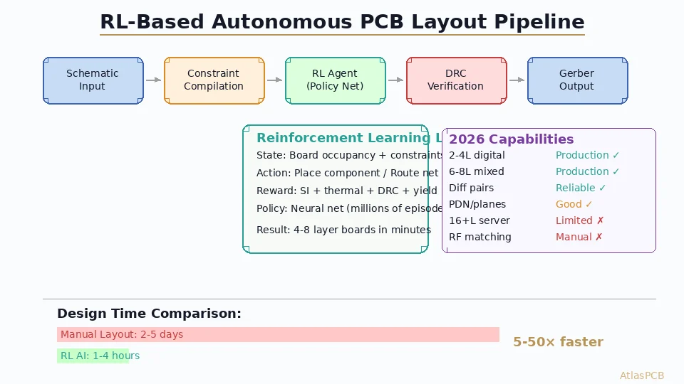
The Training Pipeline
An RL layout engine consists of several co-operating systems:
1. Environment Model (Physics Simulator)
The RL agent needs a fast, accurate model of the PCB design space. This includes:
- Board outline and keepout zones as hard constraints
- Component footprints with pin/pad geometry
- Netlist connectivity (which pins must connect)
- Layer stackup with dielectric properties
- Manufacturing rules (minimum width, spacing, via sizes)
- Electrical rules (impedance targets, max stub length, matched lengths)
The environment simulator must evaluate billions of candidate placements and routes during training, requiring extreme computational efficiency. Modern implementations use GPU-accelerated geometry engines that process 10,000+ route segments per millisecond.
2. State Representation
The agent perceives the board state through multiple encoded channels:
- Spatial occupancy maps: Which areas of each copper layer are occupied
- Thermal maps: Power dissipation density per region
- Connectivity graphs: Remaining unrouted nets and their optimal topologies
- Constraint violation maps: Areas approaching DRC limits
- Signal domain partitions: Analog vs. digital vs. power regions
This multi-channel state representation allows the agent to reason about spatial relationships, routing congestion, and constraint satisfaction simultaneously.
3. Action Space
The agent takes actions that transform the board state:
- Component placement: Selecting x, y, rotation for each component
- Route topology: Choosing which layers to use for each net
- Trace geometry: Defining width, spacing, via transitions
- Optimization moves: Ripup-and-reroute, component swapping, via minimization
The Reward Function
The reward signal is where domain expertise enters the system. A well-designed reward function balances:
R = w₁·(completeness) + w₂·(signal_integrity) + w₃·(thermal_margin)
    + w₄·(manufacturing_yield) + w₅·(area_efficiency) - penalty·(DRC_violations)
Each weight (w₁ through w₅) encodes the relative importance of different objectives. These can be tuned per application — a server board might heavily weight signal integrity while a consumer IoT device prioritizes area efficiency.
The key insight: by exposing the agent to millions of different weight combinations during training, it learns a general policy that can be conditioned on specific priorities at inference time. This is why a trained RL agent can handle diverse board types without retraining.
Constraint Compilation
Before the RL agent begins layout, the design constraints must be compiled into a format the agent can enforce:
Hard constraints (violations = invalid design):
- DRC clearances, minimum widths
- Board outline boundaries
- Mechanical keepouts (connectors, mounting holes)
- Net isolation requirements (high-voltage clearance)
Soft constraints (violations = reduced quality):
- Impedance targets (±10% acceptable)
- Length matching tolerance (±5% for DDR4)
- Component grouping preferences
- Thermal spacing recommendations
The constraint compiler translates schematic-level intent (e.g., “100Ω differential pairs on DDR bus”) into geometric rules the RL agent enforces during generation. This step is analogous to a layout engineer interpreting the EE’s design intent.
State of the Art: 2026 Capabilities
What RL Layout Can Do Today
Based on published results from Quilter, Flux AI, and academic research:
| Capability | Status | Quality Level |
|---|---|---|
| 2-layer placement + routing | Production-ready | Senior engineer equivalent |
| 4-layer mixed-signal | Production-ready | Mid-senior engineer |
| 6-8 layer digital | Beta/production | Junior-mid engineer + review |
| Component clustering | Excellent | Thermally and functionally aware |
| Differential pair routing | Reliable | <2% length mismatch |
| Power delivery network | Good | Plane splits auto-generated |
| Via minimization | Excellent | 20-40% fewer vias than manual |
| DRC compliance | >99% | Brief cleanup pass needed |
| Design time | Minutes to hours | vs. days to weeks manual |
What Still Requires Human Expertise
- 16+ layer server boards with thousands of nets and complex via stacking
- RF matching networks requiring empirical tuning of stub lengths
- High-voltage creepage/clearance in power electronics (>1kV)
- Flex-rigid transition zones with bend-radius constraints
- EMI compliance optimization for certification (FCC, CE)
- Analog layout for precision ADC/DAC and sensor interfaces
Quilter’s Project Speedrun Results
Quilter’s publicly documented autonomous layout of a complete SBC (single-board computer) demonstrated:
- Input: Schematic with ~200 components, 4-layer stackup
- Constraint compilation: Automated interpretation of design intent
- Autonomous generation: Complete placement and routing in <2 hours
- DRC result: Clean (zero violations) after brief manual pass
- Fabrication: Standard PCB fab with no special requirements
- Validation: Board powered on and ran real workloads (Linux boot, stress tests)
The board worked on first spin — a remarkable result given that many manually-laid-out prototypes require 1-3 respins to fix signal integrity or thermal issues.
Ready to Manufacture Your AI-Designed PCB?
Whether your layout comes from Quilter, Altium, or KiCad — AtlasPCB manufactures with the same precision. Our DFM review catches issues before fabrication, regardless of how the design was generated.
Upload Your Design →Implications for the PCB Manufacturing Industry
Design-to-Fabrication Compression
RL layout’s most immediate impact is on time-to-market. When layout takes minutes instead of weeks:
- Prototype iteration cycles compress from months to days
- Design exploration becomes feasible — evaluate 10 layout variants instead of 1
- Late-stage changes (component swaps, board outline modifications) become low-cost
- Concurrent engineering accelerates — mechanical and electrical design iterate simultaneously
For PCB fabricators, this means shorter quote-to-order cycles and more frequent but smaller production runs during development phases.
DFM Integration
A significant advantage of AI layout is the ability to embed manufacturing rules directly into the generation process. Rather than checking DFM after layout completion (the traditional approach), RL agents can:
- Avoid acid traps and copper slivers by construction
- Maintain minimum annular rings on all vias
- Respect panel utilization efficiency
- Generate test-point-accessible layouts
- Optimize for specific fabricator capabilities (minimum drill size, layer count constraints)
This “DFM-by-design” approach reduces fabrication issues and eliminates the back-and-forth between designer and fabricator that traditionally adds days to the NPI process.
The Human Role Evolves
RL layout doesn’t eliminate PCB engineers — it transforms their role from manual labor to design architecture and quality assurance:
Before (2020s): EE creates schematic → Layout engineer manually places and routes for 1-4 weeks → DFM review → Revisions
After (2026+): EE creates schematic → AI generates candidate layouts in hours → Engineer reviews, selects best variant, applies domain-specific refinements → DFM passes automatically
The engineer’s expertise shifts from “how to route this differential pair” (solved by AI) to “what constraints should I specify” and “is this result good enough” (judgment and architecture).
Technical Challenges and Limitations
The Generalization Problem
RL agents trained on one class of boards (e.g., 4-layer digital) may not perform well on fundamentally different topologies (e.g., high-power motor drives). Current solutions:
- Train on diverse board populations (10,000+ real designs)
- Use transfer learning from simpler to complex topologies
- Employ curriculum learning (progressively harder boards during training)
- Allow human constraint injection to guide unfamiliar scenarios
Verification Trust
Engineers rightfully question whether AI-generated layouts satisfy intent, not just rules. A layout can be DRC-clean yet have poor signal integrity or thermal hotspots. Verification requires:
- Post-layout SI simulation (eye diagrams, S-parameters)
- Thermal analysis (CFD or finite-element)
- EMI prediction (near-field radiation patterns)
- Manufacturing yield analysis (process capability vs. feature sizes)
The verification stack remains human-directed, even as generation becomes automated.
IP and Liability
When an AI generates a layout that later fails in the field, the liability chain is unclear. Industry standards bodies (IPC, JEDEC) have not yet addressed AI-generated designs in their certification frameworks. This is an active area of discussion in the EDA community.
Key Takeaways
- RL layout is production-real in 2026 — Quilter and others have demonstrated first-spin-success on real hardware
- 4-8 layer boards up to 500 components are within current AI capability
- Time compression is the primary value — minutes vs. weeks for layout generation
- Human review remains essential for verification, constraint specification, and edge cases
- Manufacturing doesn’t change — AI-generated Gerbers fabricate identically to human-generated ones
The AI revolution in PCB design is here. The question for hardware teams is no longer “if” but “when” to integrate autonomous layout into their workflow.
Further Reading
- Quilter AI Autonomous PCB Layout: Project Speedrun Analysis
- Siemens Fuse EDA AI Agent for PCB Workflow Orchestration
- Text-to-PCB: Generative AI Design Disruption
AtlasPCB manufactures PCBs from any EDA tool output — including AI-generated designs. Our DFM review ensures manufacturability regardless of how your layout was created. Get a quote for your next project.
About AtlasPCB — We specialize in complex PCB manufacturing for HDI, RF, and high-reliability applications. Explore our full PCB manufacturing capabilities, or get an instant online quote . Every order includes free engineering review. Get your quote.
Reviewed by AtlasPCB Engineering Team — IPC-certified manufacturing specialists with 15+ years of production experience in HDI, RF, and high-reliability PCB fabrication. Content based on factory floor data and real customer design reviews.
- AI PCB design
- reinforcement learning
- autonomous layout
- EDA automation
- hardware AI
- Quilter
- PCB routing