· AtlasPCB Engineering · Engineering · 12 min read
Rigid-Flex PCB Design Guide: Bend Radius, Layer Transitions, and Reliability for Wearables and Aerospace
Complete rigid-flex PCB design guide covering bend radius calculations, flex-to-rigid transition zones, copper type selection, coverlay vs solder mask, IPC-2223 compliance, and reliability testing for dynamic and static flex applications.

Introduction: Why Rigid-Flex PCBs Are Everywhere
From the Apple Watch on your wrist to satellite solar array controllers orbiting Earth, rigid-flex PCBs have become indispensable wherever electronics must be compact, lightweight, and mechanically complex. By combining rigid board sections (for component mounting and connectors) with flexible polyimide circuits (for interconnection and folding), rigid-flex eliminates connectors, reduces assembly steps, and enables three-dimensional packaging impossible with traditional rigid boards.
The global rigid-flex market is growing at 12% CAGR, driven by:
- Consumer wearables: Smartwatches, AR glasses, hearing aids
- Medical devices: Implantables, endoscopes, surgical robots
- Aerospace/defense: Satellite electronics, missile guidance, conformal antennas
- Automotive: ADAS camera modules, battery management systems
- Industrial: Robotics, test equipment, instrumentation
But rigid-flex design is unforgiving. Unlike rigid PCBs where most design rules have generous margins, flex circuits operate near material limits. A bend radius just slightly too tight, copper type wrongly specified, or transition zone poorly designed will cause catastrophic failure—either immediately during assembly or insidiously after thousands of flex cycles in the field.
This guide covers everything you need to design reliable rigid-flex PCBs, from fundamental material physics through production-proven design rules and IPC compliance. For related content, see our comparison of [rigid vs flexible PCBs]/blog/rigid-vs-flexible-pcb/) and our [HDI any-layer PCB design guide]/blog/any-layer-hdi-pcb-design-wearable-sip/) for designs combining rigid-flex with microvia technology.
Rigid-Flex Construction Fundamentals
Basic Stackup Architecture
A rigid-flex PCB consists of three zone types:
Rigid Zones: Standard FR-4 or high-Tg laminate with full copper layer stack, solder mask, and surface finish. Components are mounted here. Typical thickness: 0.8-2.4 mm.
Flex Zones: Polyimide (Kapton or equivalent) base film with copper traces, covered by polyimide coverlay. This section bends. Typical thickness: 0.1-0.4 mm per flex layer.
Transition Zones: Where rigid meets flex. The most failure-prone area in any rigid-flex design. Requires careful geometric and material management.
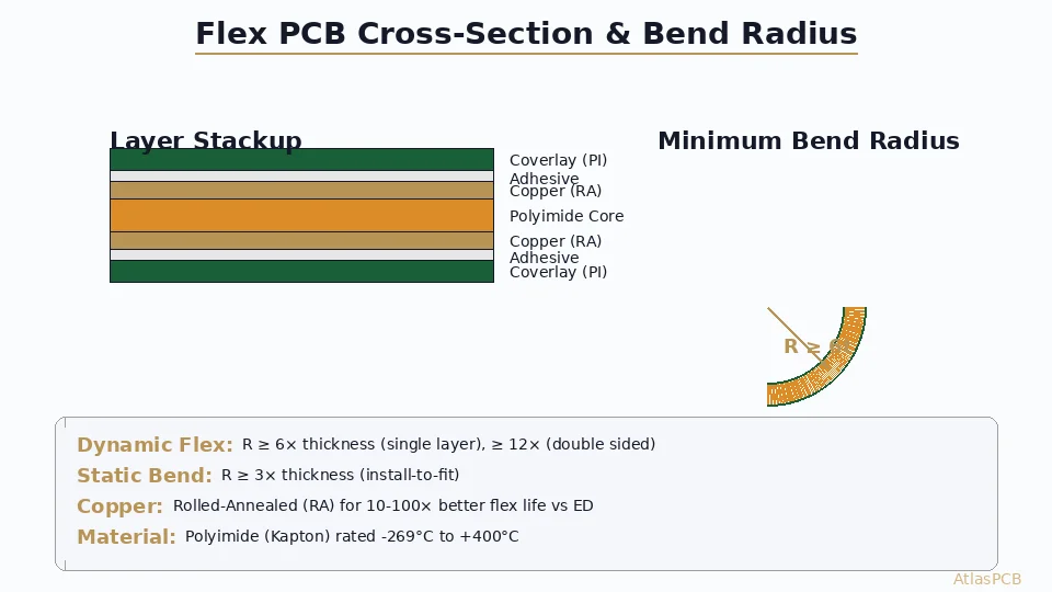
Material Stack in Flex Zone
A typical 2-layer flex section:
Coverlay polyimide (12.5-25 μm)
Coverlay adhesive (12.5-25 μm)
Copper Layer 1 - RA copper (12-35 μm)
Polyimide base film (12.5-50 μm)
Copper Layer 2 - RA copper (12-35 μm)
Coverlay adhesive (12.5-25 μm)
Coverlay polyimide (12.5-25 μm)
Total flex thickness: 0.1-0.2 mm for 2-layer construction
Adhesiveless vs. Adhesive-Based Construction
Adhesive-based (3-layer): Polyimide + adhesive (acrylic/epoxy) + copper. Lower cost, wider availability, standard construction. Adhesive layer limits temperature capability to ~120°C continuous.
Adhesiveless (2-layer): Copper directly deposited or laminated onto polyimide without adhesive. Higher temperature capability (200°C+), thinner construction, better dimensional stability. Required for HDI flex and aerospace applications.
Bend Radius: The Critical Design Parameter
Bend Radius Defined
Bend radius (R) is measured from the inside surface of the bend to the neutral axis of the flex circuit. For a uniform flex section:
Neutral axis location = center of the flex thickness (for symmetric constructions)
Key formula: Strain at outer copper layer = t / (2R + t)
Where t = total flex thickness and R = bend radius to inside surface.
For copper to survive without cracking, strain must remain below the material’s fatigue endurance limit:
- RA copper elongation limit (static): ~15-20%
- RA copper fatigue limit (dynamic, 10⁶ cycles): ~0.3-0.5%
- ED copper elongation limit: ~8-12% (avoid for flex)
Minimum Bend Radius Table
| Configuration | Static Bend (1× fold) | Dynamic Bend (> 100 cycles) |
|---|---|---|
| 1-layer flex (50 μm total) | 6× t = 0.3 mm | 12× t = 0.6 mm |
| 2-layer flex (150 μm total) | 8× t = 1.2 mm | 20× t = 3.0 mm |
| 3-layer flex (250 μm total) | 10× t = 2.5 mm | 22× t = 5.5 mm |
| 4-layer flex (350 μm total) | 12× t = 4.2 mm | 25× t = 8.75 mm |
Note: These are minimum values. Add 50% safety margin for production designs.
Factors That Increase Required Bend Radius
- Thicker copper: 1 oz (35 μm) vs ½ oz (18 μm) copper doubles the strain
- Copper on outside of bend: Outer surface experiences tensile strain (worst case)
- Stacked traces: Copper on multiple layers aligned vertically creates a thicker effective section
- Plated features in flex zone: Plated through-holes add rigid elements that concentrate stress
- Temperature extremes: Cold temperatures reduce copper ductility
- Contamination/handling damage: Surface scratches become crack initiation sites
Dynamic Flex Design Rules
For applications requiring repeated bending (hinges, printer heads, robot cables):
- Single-layer flex preferred: Minimize flex section layer count
- ½ oz RA copper only: Never use 1 oz or ED copper in dynamic zones
- Bend radius > 20× thickness: Conservative for millions of cycles
- No plated features in bend zone: PTH, vias, and plated pads are rigid inclusions that crack
- Symmetrical copper distribution: Equal copper on both sides of neutral axis
- Stagger traces: Offset traces between layers so they don’t stack (see section below)
- Curved traces through bend: Route traces perpendicular to bend axis; avoid routing parallel
Transition Zone Design: Where Failures Start
The rigid-to-flex transition is statistically the most common failure point in rigid-flex PCBs. Stress concentrates at this boundary because:
- Material stiffness changes abruptly (FR-4 modulus: 20 GPa → polyimide: 3 GPa)
- Copper traces must cross from supported (rigid) to unsupported (flex) regions
- Manufacturing processes create localized stress (adhesive squeeze-out, coverlay termination)
Transition Zone Geometry
Correct: Graduated Transition
    Rigid Section         Transition         Flex Section
    ═══════════════╗                      ╔══════════════
                    ╲    30-45° angle    ╱
    ═══════════════╝                      ╚══════════════
                   ←── 1.5-3 mm ──→
Wrong: Sharp 90° Transition
    Rigid Section     │    Flex Section
    ═════════════════║═══════════════════
    ═════════════════║═══════════════════
                     │
              Stress concentration!
Design Rules for Transition Zones
Taper angle ≤ 45°: Bookshelf-style rigid section edges reduce stress concentration by 60% compared to vertical edges
Stress-relief features: Add teardrop-shaped cutouts (relief slots) in the flex material at the transition point. Typically 0.5-1.0 mm diameter half-circles at the rigid edge corners.
Coverlay extension: Extend coverlay 1-2 mm into the rigid section to prevent delamination initiation at the boundary
No components within 2 mm of transition: Component pads and solder joints near the flex boundary experience fatigue from micro-flexing
Anchor copper pads: Place non-functional copper pads (hatched ground fill) in the flex zone immediately adjacent to the transition to distribute stress
Through-hole keep-out: No PTH vias within 1.5 mm of the rigid-to-flex transition line
Rigid-Flex PCB Manufacturing
AtlasPCB fabricates 1-8 layer rigid-flex with polyimide flex zones, RA copper, and IPC-2223 compliant transition design. We handle aerospace, medical, and consumer wearable applications.
Get Rigid-Flex Quote →Copper Routing in Flex Zones
Perpendicular Routing Rule
Always route traces perpendicular to the bend axis. This is the single most important routing rule for flex circuits.
When traces run perpendicular to the bend, each individual conductor experiences uniform strain distributed along its width. When traces run parallel to the bend axis, they experience concentrated tensile/compressive stress along their length, with strain localized at the bend entry/exit points.
Trace Staggering Between Layers
For multi-layer flex sections, never align (stack) traces on different layers:
Correct (staggered):
Layer 1:  ─── ─── ─── ─── (traces)
Layer 2:    ─── ─── ─── ─── (offset by half pitch)
Wrong (stacked):
Layer 1:  ─── ─── ─── ─── (traces)
Layer 2:  ─── ─── ─── ─── (directly below)
Stacked traces create localized thickness increases (I-beam effect) that resist bending and concentrate stress at the trace edges.
Hatched Ground Planes in Flex
Solid copper planes in flex zones are problematic:
- Increase effective thickness and stiffness
- Resist bending uniformly rather than allowing flex
- Can delaminate from polyimide if adhesion is marginal
Solution: Use hatched (crosshatch) ground fills:
- 45° hatch angle relative to bend axis
- Conductor width: 0.1-0.15 mm
- Opening size: 0.5-1.0 mm
- Results in ~40-60% copper coverage (vs. 100% solid)
- Provides adequate shielding while maintaining flexibility
- Shield effectiveness is ~20 dB less than solid plane at GHz frequencies
Trace Width Considerations
Wider traces have better flex fatigue resistance than narrow traces:
- Narrow traces (< 75 μm) concentrate strain at edges
- Wide traces (> 200 μm) distribute strain more uniformly
- Minimum recommended trace width in dynamic flex zone: 100 μm (4 mil)
- For high cycle count applications: 150 μm (6 mil) minimum
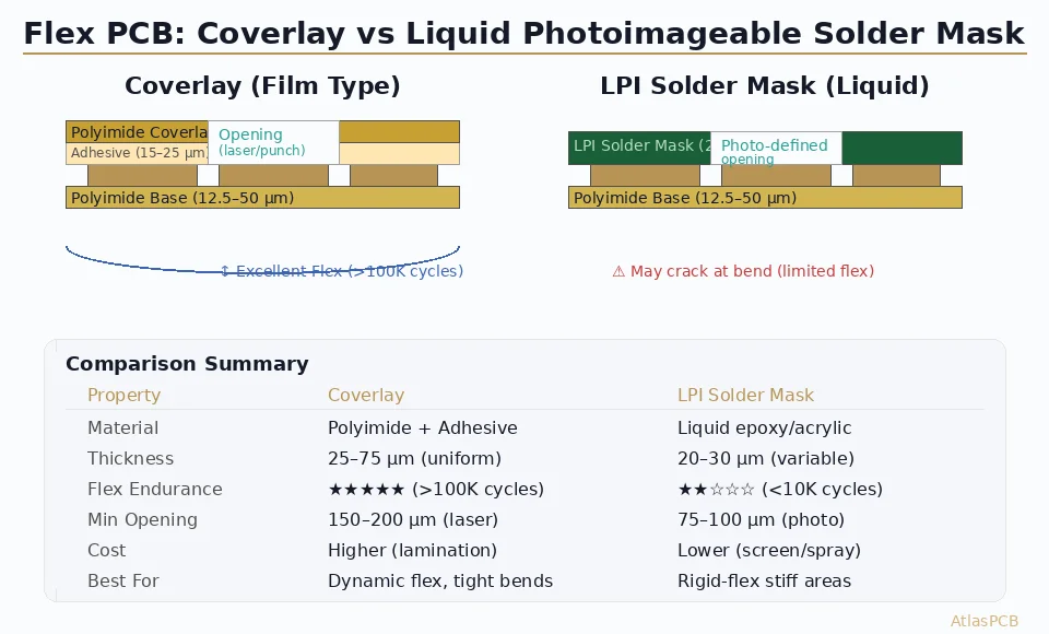
Polyimide and Coverlay Selection
Base Film Materials
Standard polyimide (Kapton HN equivalent):
- Thickness: 12.5, 25, 50 μm
- Tensile strength: 230 MPa
- Elongation: 70%
- Temperature range: -269°C to +400°C
- Moisture absorption: 2.9% (at 50% RH)
- Dk: 3.4 @ 1 MHz
Modified polyimide (Kapton EN):
- Lower moisture absorption (1.8%)
- Better dimensional stability
- Preferred for HDI flex and impedance-controlled designs
- Cost premium: ~20%
Coverlay vs. Flexible Solder Mask
| Feature | Coverlay (PI film) | Flex Solder Mask |
|---|---|---|
| Bend fatigue life | Excellent (>10⁶ cycles) | Fair (cracks at 10⁴ cycles) |
| Opening tolerance | ±75 μm | ±25 μm |
| Min opening size | 200 μm | 75 μm |
| Temperature capability | 300°C+ | 150°C |
| Application method | Die-cut + laminate | Photo-image + develop |
| Flexibility | Maintains flex performance | Restricts bending slightly |
| Cost | Higher (die-cut tooling) | Lower (standard process) |
Recommendation: Use coverlay in all flex zones that will be bent. Use flex solder mask only in flat flex areas that need fine-pitch pad exposure.
IPC-2223 Design Standard Compliance
IPC-2223 (Sectional Design Standard for Flexible Printed Boards) defines requirements for flex and rigid-flex design. Key requirements:
Conductor Spacing in Flex
- Minimum conductor spacing: 75 μm (Class 2), 50 μm (Class 3)
- Spacing from conductor to flex board edge: 0.5 mm minimum
- Conductor-to-bend area: No width changes within the bend radius zone
Annular Ring Requirements
- PTH in rigid zones: Standard IPC-2221 applies (50 μm Class 2)
- Pads in flex zones: Anchoring features required
- Tear-drop entry to pads
- Minimum pad-to-conductor transition radius: 0.2 mm
- No acute angles in copper geometry
Bend Area Requirements
- No plated through-holes in bend areas
- No component mounting in bend areas
- Minimum distance from bend to nearest PTH: 2.5 mm
- Strain relief required at cable terminations
Testing Requirements per IPC-2223
- Flex endurance test (dynamic): IPC-TM-650 Method 2.4.3 — cycle at rated bend radius until failure, minimum life specified
- Thermal shock: -65°C to +125°C, 100 cycles, no visible damage
- Peel strength: Copper-to-polyimide > 0.7 N/mm after conditioning
- Impedance: ±10% of nominal after flex cycling (for controlled impedance flex)
Common Applications and Design Examples
Consumer Wearable (Smartwatch)
Requirements:
- 6-layer rigid (2 rigid sections for display and sensor boards)
- 2-layer flex (connecting display to main board)
- 180° fold (static during assembly)
- Total package height: < 4 mm
Design approach:
- Flex section: 2-layer, 50 μm PI, ½ oz RA copper, coverlay both sides
- Flex thickness: 0.2 mm → bend radius: 8× = 1.6 mm (static)
- Transition: 30° taper with stress relief slots
- Impedance-controlled differential pairs (100 Ω) for display MIPI interface
Aerospace Satellite Electronics
Requirements:
- 12-layer rigid (4 rigid sections for processing modules)
- 4-layer flex (connecting modules across deployment mechanism)
- Dynamic flex: 90° bend, 500 deployment cycles over 15-year life
- Temperature: -180°C to +150°C (eclipse to sun exposure)
- Radiation: 50 krad TID tolerance (material selection)
Design approach:
- Flex section: 2-layer flex (only 2 of the 4 layers extend through flex; rest terminate)
- Adhesiveless construction (no organic adhesive Tg limitation)
- 18 μm RA copper, 50 μm Kapton HN base
- Flex thickness: 0.15 mm → bend radius: 25× = 3.75 mm (dynamic, with margin)
- Conformal coat flex section with Parylene C for outgassing protection
- Staked (anchored) connectors at rigid boundaries
Medical Endoscope
Requirements:
- 4-layer rigid (camera module at tip)
- 1-layer flex (runs full length of scope shaft, 1.5 m)
- Dynamic flex: continuous articulation, >50,000 cycles
- Diameter constraint: flex must fit inside 3 mm tube
- Sterilization: withstand autoclave (134°C, 18 min, 1000 cycles)
Design approach:
- Single-layer flex with ½ oz RA copper, adhesiveless
- Flex thickness: 0.05 mm → bend radius: 25× = 1.25 mm (adequate for 3mm tube)
- Gold plating on flex for corrosion resistance in humid/steam environment
- Helical trace routing to distribute strain uniformly
- No ground plane in flex—use twisted pair geometry for EMI control
Manufacturing Considerations
Fabricator Selection Criteria
Not all PCB fabricators can produce rigid-flex. Key capabilities to verify:
- Sequential lamination: Rigid-flex requires multiple lamination cycles
- Polyimide processing: Different drilling, plating, and handling vs FR-4
- RA copper sourcing: Must stock or reliably source rolled annealed copper foils
- Coverlay registration: Die-cutting or laser-cutting coverlay openings with ±75 μm accuracy
- Flex handling: Clean room processing to prevent contamination between layers
- Cross-section capability: Must verify bend zone construction on first articles
- Flex testing: In-house IPC-TM-650 flex endurance testing
Lead Time and Cost Expectations
Rigid-flex PCBs are significantly more expensive and slower than standard rigid boards:
- Prototype lead time: 3-4 weeks (vs 5-7 days for standard rigid)
- Production lead time: 4-6 weeks (vs 2-3 weeks for rigid)
- Cost multiplier: 3-8× equivalent rigid board (depending on complexity)
- First article verification: Essential—always order 3-5 bare boards for cross-section and bend testing before production
Design for Manufacturing Tips
- Keep flex zones short: Every mm of flex adds cost and reduces yield
- Minimize flex layer count: 1-2 layers if possible
- Standard materials: Use common polyimide/copper thicknesses for shorter lead times
- Panel layout: Rigid-flex utilizes panels poorly—expect 30-60% utilization vs 80%+ for rigid
- Test coupons: Include flex bend test coupons and peel strength coupons in panel border
- Clear documentation: Call out flex/rigid zones, bend direction, and installed configuration in fabrication drawing
Reliability Testing Protocol
Before committing a rigid-flex design to production, validate with these tests:
Recommended Test Sequence
- Visual/dimensional inspection (IPC-6013)
- Microsection at transition zones (verify construction matches design)
- Bend endurance (IPC-TM-650 2.4.3): Cycle at rated bend radius
- Static applications: 10 cycles to verify no damage
- Dynamic applications: 2× rated cycle life minimum
- Thermal cycling (IPC-TM-650 2.6.7): -55°C to +125°C, 500 cycles
- Solder float (IPC-TM-650 2.4.13): 288°C for 10 seconds, 3 cycles
- Peel strength (IPC-TM-650 2.4.9): Before and after conditioning
- Impedance verification: TDR measurement through flex zone before and after flex cycling
- Continuity under flex: Monitor resistance while cycling (detects intermittent opens)
Conclusion: Design for the Fold
Rigid-flex PCB design demands respect for material physics that rigid-only designers rarely encounter. The flex zone operates near material limits by definition—there’s no generous safety margin that forgives sloppy design.
The essential principles:
- Use RA copper in every flex zone, no exceptions
- Calculate bend radius properly and add margins
- Design transition zones with graduated geometry
- Route perpendicular to bend, stagger between layers
- Specify coverlay for any zone that will flex
- Test early with real bend cycling, not just simulation
Get these fundamentals right, and rigid-flex delivers extraordinary design freedom. Get them wrong, and you’ll discover failures at the worst possible time—in the field, after shipping thousands of units.
Planning a rigid-flex design? AtlasPCB’s engineering team reviews flex zone construction, validates bend radius calculations, and provides DFM feedback specific to your application. We’ve fabricated rigid-flex for medical, aerospace, and consumer wearable customers worldwide. Start your rigid-flex project with confidence.
Further Reading
- [PCB Rigid-Flex Bend Zone Reliability: Design Rules, Material Selection & Lifecycle Testing]/blog/pcb-rigid-flex-bend-zone-reliability/)
- [ENEPIG vs ENIG Surface Finish: Complete Comparison for Wire Bonding, Solderability, and Long-Term Reliability]/blog/enepig-vs-enig-surface-finish-wire-bonding/)
- [PCB Surface Finish Comparison: OSP vs HASL vs Immersion Silver vs ENIG for Assembly Reliability]/blog/pcb-surface-finish-osp-hasl-enig-immersion-silver-comparison/)
- [ENEPIG vs ENIG: Which PCB Surface Finish for Your Design?]/blog/enepig-vs-enig/)
- [PCB Surface Finish Selection — ENIG vs HASL vs OSP vs Hard Gold vs ENEPIG]/blog/pcb-surface-finish-enig-hasl-osp-hard-gold-enepig/)
- Rigid PCB Manufacturing
About AtlasPCB — We specialize in complex PCB manufacturing for HDI, RF, and high-reliability applications. Explore our rigid-flex PCB manufacturing, free engineering DFM review, or get an full PCB manufacturing capabilities . Every order includes free engineering review. Get your quote.
Reviewed by AtlasPCB Engineering Team — IPC-certified manufacturing specialists with 15+ years of production experience in HDI, RF, and high-reliability PCB fabrication. Content based on factory floor data and real customer design reviews.
- rigid-flex PCB
- flex PCB
- bend radius
- polyimide
- coverlay
- IPC-2223
- wearable electronics
- aerospace PCB
- dynamic flex
- DFM