· AtlasPCB Engineering · Engineering · 8 min read
BGA Pad Cratering: Root Causes, IPC-9708 Testing, and PCB Design Mitigations
Complete engineering guide to BGA pad cratering in PCB assemblies. Covers fracture mechanics, IPC-9708 ball pull/shear testing, laminate selection, pad design strategies, and prevention methods for high-reliability electronics.

Understanding BGA Pad Cratering
Ball Grid Array (BGA) packages dominate modern electronics — from smartphones to server motherboards. As the industry transitioned to lead-free soldering under RoHS, a new failure mode emerged that was rarely seen with tin-lead solder: pad cratering.
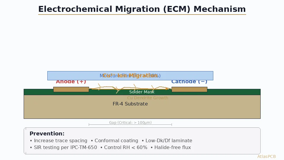
Pad cratering is a fracture that occurs within the PCB laminate resin directly beneath a copper pad. Unlike a clean pad lift where copper peels from the substrate surface, cratering involves a sub-surface crack that propagates through the glass-fiber-reinforced epoxy, often exposing bare glass weave fibers. This failure is particularly insidious because it can be electrically intermittent — the circuit may pass initial testing but fail under subsequent mechanical or thermal stress.
The root cause lies in the fundamental material property mismatch introduced by lead-free assembly. SAC305 solder (Sn96.5/Ag3.0/Cu0.5) has a significantly higher elastic modulus (~50 GPa) compared to SnPb eutectic (~30 GPa). This stiffer solder joint transfers more mechanical energy to the pad-laminate interface during impact or flexure events, rather than absorbing it through plastic deformation as SnPb did.
Fracture Mechanics of Pad Cratering
Stress Distribution at the Pad Interface
When a BGA assembly experiences mechanical loading (board-level drop, bend, or thermal cycling), the solder joints transfer forces to the PCB pads. The critical stress concentration occurs at the pad periphery — the boundary where copper, solder mask, and laminate resin converge.
For a circular pad of diameter d under pure tensile loading, the maximum peel stress σ_max at the pad edge is approximately:
σ_max ≈ F / (π × d × t_Cu)
Where F is the applied force, d is pad diameter, and t_Cu is copper thickness. However, the actual failure mode is more complex — it involves mixed-mode (Mode I + Mode II) fracture where both peel (tensile) and shear components contribute.
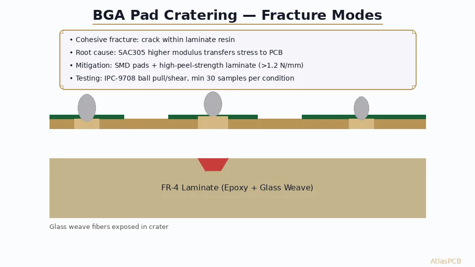
Three Critical Fracture Paths
Cohesive fracture within laminate — Crack propagates through the resin matrix between glass fiber bundles. This is true pad cratering and indicates the laminate’s fracture toughness (G_IC) was exceeded.
Adhesive fracture at copper-resin interface — Separation at the boundary between the copper foil treatment and resin. Often related to insufficient surface roughness (tooth profile) on the copper foil.
Mixed-mode fracture — Crack initiates at the interface and then deviates into the laminate bulk, or vice versa. Most real-world failures exhibit mixed-mode behavior.
Why Lead-Free Makes It Worse
The transition from SnPb to SAC alloys fundamentally changed the load path mechanics:
| Parameter | SnPb Eutectic | SAC305 |
|---|---|---|
| Elastic modulus | ~30 GPa | ~50 GPa |
| Yield strength | ~25 MPa | ~40 MPa |
| Creep compliance | High | Low |
| Energy absorption | Solder deforms | PCB absorbs stress |
With SnPb solder, the joint itself acted as a mechanical fuse — deforming plastically before stress could damage the PCB. SAC305’s higher stiffness and strength means the solder ball transmits mechanical energy directly to the pad-laminate interface, essentially making the PCB the weakest link in the chain.
IPC-9708 Testing Methodology
Test Overview
IPC-9708 (“Test Method for Evaluating the Susceptibility of Printed Board Assemblies to Pad Cratering”) was developed specifically to quantify pad cratering risk. It defines two primary test methods:
Ball Pull Test:
- Apply controlled upward force on individual solder balls
- Record maximum force at failure
- Speed: 5 mm/s (standard) or 0.5 mm/s (quasi-static)
- Sample size: minimum 30 balls per condition
Ball Shear Test:
- Apply lateral shear force to solder balls at a fixed height
- Shear tool height: 25% of ball height above the board surface
- Speed: 100-1000 µm/s
- Sample size: minimum 30 balls per condition
Failure Mode Classification
After testing, each failure site is examined under optical microscopy (50-100×) and classified:
- Mode 1: Solder joint failure (cohesive within solder) — Not a cratering issue
- Mode 2: Interface failure between solder and pad — Soldering process issue
- Mode 3: Pad lift (adhesive failure at copper-resin interface) — Cratering precursor
- Mode 4: Pad cratering (cohesive failure in laminate) — True cratering
- Mode 5: Trace/conductor failure — Design issue
A cratering rate above 5% in ball pull testing is generally considered unacceptable for high-reliability applications (automotive, aerospace, medical). Consumer electronics may tolerate up to 15% depending on the severity depth and end-use environment.
Advanced Characterization
Beyond IPC-9708 basic testing, comprehensive cratering evaluation includes:
- Cross-sectioning: Microsection through crater sites to measure crack depth and propagation direction
- Dye-and-pry: Fluorescent dye penetrant reveals crack extent before mechanical separation
- Acoustic microscopy (C-SAM): Non-destructive detection of subsurface delamination
- SEM/EDS: Elemental analysis of fracture surface to confirm failure location
Need Pad Cratering Testing for Your BGA Design?
AtlasPCB offers IPC-9708 qualified laminate testing and optimized stackup designs to eliminate pad cratering risk in your high-reliability assembly.
Request Engineering Review →PCB Design Strategies to Prevent Pad Cratering
1. Laminate Material Selection
The single most effective mitigation is choosing a laminate with high fracture toughness. Key material properties to evaluate:
Peel strength (IPC-TM-650 2.4.8):
- Standard FR-4: 0.7-1.0 N/mm
- Enhanced resin systems: 1.2-1.8 N/mm
- High-performance (Megtron 6, IS415): 1.4-2.0 N/mm
T-288 (time to delamination at 288°C):
- Minimum for lead-free: >5 minutes
- Recommended: >15 minutes
- Indicates thermal robustness of resin-copper bond
Tg and Td:
- Higher Tg (>170°C) and Td (>340°C) laminates generally exhibit better fracture resistance
- The filler content and resin chemistry affect crack propagation energy
Specific material recommendations for BGA-intensive designs:
- Isola IS415/IS420 — Enhanced resin system with superior peel strength
- Panasonic Megtron 6 — Low-loss with high pad adhesion
- Shengyi S1000-2M — Cost-effective enhanced FR-4
- Nelco N4000-13 EP — High fracture toughness epoxy system
2. Pad Geometry Optimization
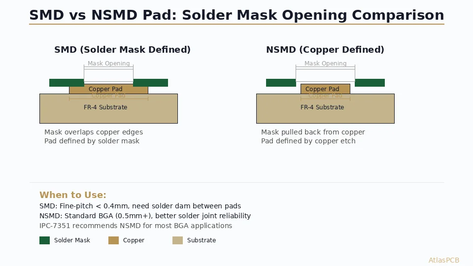
Solder-Mask-Defined (SMD) vs Non-Solder-Mask-Defined (NSMD):
NSMD pads (copper-defined) are standard for BGAs because they allow larger solder joint volumes and self-centering during reflow. However, SMD pads provide superior cratering resistance because the solder mask:
- Reinforces the pad perimeter against peel forces
- Distributes stress over a larger interface area
- Prevents crack initiation at the pad edge
Hybrid approach for critical BGAs:
- Use SMD pads for corner and edge balls (highest stress during drop/bend)
- Use NSMD for center balls (lower stress, need alignment accuracy)
- This reduces cratering risk by 40-60% versus all-NSMD designs
Pad size considerations:
- Smaller pads concentrate force over less laminate area — lower absolute stress
- However, smaller pads require tighter registration tolerances
- Optimal: Match pad diameter to BGA ball pitch minus 20% (e.g., 0.5mm pitch → 0.4mm pad)
3. Copper Foil Treatment
The microscopic surface profile (tooth) of the copper foil dramatically affects adhesion:
- Standard electrodeposited (ED) copper: 5-8 µm tooth height — adequate for most applications
- High-profile (HP) copper: 8-12 µm tooth — 30-50% better adhesion to resin
- Reverse-treated foil (RTF): Treatment on both sides — best for embedded applications
- Very low profile (VLP): <3 µm tooth — worst for cratering resistance (avoid for large BGAs)
For BGA-intensive designs, specify at minimum standard-profile copper foil (not VLP/HVLP) on layers directly beneath BGA pads.
4. Stackup Design
- Copper thickness under BGA: 1 oz (35µm) minimum; 0.5 oz (18µm) increases cratering risk
- Prepreg selection: Higher resin content prepreg (≥55% RC) between layers provides more fracture-resistant interlayer bonding
- Glass weave style: 1080 glass weave has finer bundles than 7628, providing more uniform resin distribution and fewer crack propagation paths
- Symmetrical stackup: Prevents residual stress from warpage that pre-loads pad interfaces
5. Assembly Process Optimization
- Reflow profile: Minimize time above liquidus (TAL) — longer TAL degrades the copper-laminate interface. Target 60-90 seconds for SAC305.
- Peak temperature: Keep below 245°C if possible; each degree above 240°C accelerates intermetallic growth and interface weakening
- Cooling rate: 2-4°C/s cooling produces finer grain structure in SAC solder, slightly reducing impact force transmission
- Board support during reflow: Adequate support prevents warpage-induced pre-stress on pad interfaces
Real-World Case Studies
Case 1: Automotive ECU Drop Test Failure
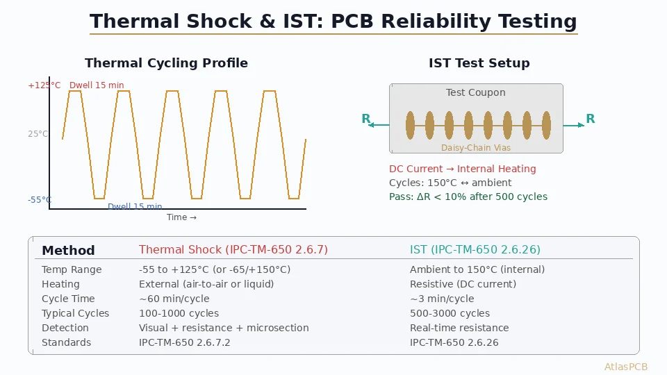
A Tier-1 automotive supplier experienced 12% pad cratering rate on a 0.8mm pitch BGA during 1500G drop testing per JEDEC JESD22-B111. Root cause analysis revealed:
- Standard FR-4 (Tg 150°C) with VLP copper foil
- All NSMD pads on the BGA
- Peak reflow temperature of 250°C
Solution: Switching to IS415 laminate with standard ED copper, converting corner pads to SMD, and reducing peak temperature to 242°C eliminated all cratering failures through 30 drops.
Case 2: Server Motherboard Thermal Cycle Failure
A server OEM found intermittent BGA connections after 500 thermal cycles (-40°C to +125°C). Cross-sections revealed shallow craters (20-30µm deep) at 0.4mm pitch BGA corners.
Solution: Increased copper weight from 0.5 oz to 1 oz on the BGA layer, specified high-peel-strength prepreg (>1.4 N/mm), and added solder mask reinforcement at corner pad positions. Zero failures through 1000 cycles.
Testing and Qualification Workflow
For any new BGA design destined for harsh environments, the recommended qualification flow is:
- Material screening: Request IPC-9708 ball pull data from laminate supplier for your specific copper foil + prepreg combination
- Design prototype: Build test coupons with candidate designs (NSMD, SMD, hybrid)
- Baseline testing: Perform ball pull/shear on as-reflowed samples to establish baseline
- Environmental stress: Subject test vehicles to relevant conditions (thermal cycling, drop, or bend per your product requirements)
- Post-stress testing: Repeat ball pull/shear and compare failure mode distribution
- Production monitoring: Implement periodic ball pull testing as part of incoming quality control
Industry Standards Reference
| Standard | Coverage |
|---|---|
| IPC-9708 | Pad cratering test method |
| IPC-TM-650 2.4.8 | Peel strength testing |
| JEDEC JESD22-B111 | Board-level drop testing |
| IPC-SM-785 | Solder joint reliability guidelines |
| IPC-7095 | BGA design and assembly guidelines |
| IPC-A-610 Class 3 | Acceptability criteria for high-reliability |
Key Takeaways
BGA pad cratering is a predictable, preventable failure mode when addressed at the design stage. The three highest-impact mitigations are:
- Select high-peel-strength laminate (>1.2 N/mm) with appropriate Tg/Td for your reflow profile
- Use SMD or hybrid pad definitions for mechanically-stressed BGA positions
- Specify standard-profile (not VLP) copper foil on BGA pad layers
For safety-critical applications, IPC-9708 qualification testing should be a standard part of your design validation process — not an afterthought when field failures occur.
Further Reading
- Via-in-Pad Plated Over (VIPPO) Design Guide
- IPC-A-610 Class 3 Inspection Requirements
- PCB Reflow Soldering Profile Optimization
AtlasPCB manufactures BGA-optimized PCBs with IPC-9708 qualified laminates and advanced pad designs for automotive, aerospace, and medical applications. Get a quote for your high-reliability BGA design.
About AtlasPCB — We specialize in complex PCB manufacturing for HDI, RF, and high-reliability applications. Explore our HDI PCB manufacturing capabilities, or get an full PCB manufacturing capabilities . Every order includes free engineering review. Get your quote.
Reviewed by AtlasPCB Engineering Team — IPC-certified manufacturing specialists with 15+ years of production experience in HDI, RF, and high-reliability PCB fabrication. Content based on factory floor data and real customer design reviews.
- BGA
- pad cratering
- IPC-9708
- PCB reliability
- lead-free assembly
- laminate fracture
- high-reliability PCB