· AtlasPCB Engineering · Engineering · 4 min read
PCBA Assembly Process: From Bare Board to Finished Product
Understand the complete PCB assembly (PCBA) process — solder paste printing, pick and place, reflow soldering, wave soldering, inspection, and functional testing explained step by step.

PCB Assembly (PCBA) is the process of soldering electronic components onto a bare PCB to create a functional circuit board. This guide walks through each step of the modern PCBA manufacturing process.
Step 1: Solder Paste Printing
Solder paste — a mixture of tiny solder balls (25-45um diameter) suspended in flux — is deposited onto the PCB pads through a stainless steel stencil.
Process Details
- Stencil: Laser-cut stainless steel sheet (typically 0.10-0.15mm thick) with apertures matching pad locations
- Printer: Automated screen printer aligns the stencil to the board using fiducial marks
- Squeegee: Metal or polyurethane blade pushes paste across the stencil at controlled speed and pressure
- Paste volume: Critical parameter — too little causes insufficient solder, too much causes bridging
Key Parameters
| Parameter | Typical Value |
|---|---|
| Stencil thickness | 0.10mm (fine-pitch), 0.12mm (standard), 0.15mm (large pads) |
| Squeegee speed | 25-75mm/s |
| Squeegee pressure | 3-8 kg |
| Print accuracy | +/-0.025mm |
| Cycle time | 15-30 seconds/board |
Solder Paste Inspection (SPI)
After printing, 3D SPI systems measure paste volume, height, and area on every pad. This catches ~60% of all assembly defects at the earliest possible stage.
Step 2: Component Placement (Pick and Place)
Automated pick-and-place machines place SMD components onto the solder paste with extreme precision.
Machine Types
- Chip shooter: High-speed placement of small passives (resistors, capacitors). Speed: 40,000-80,000 CPH.
- Fine-pitch placer: Precision placement of ICs, BGAs, QFPs. Speed: 10,000-30,000 CPH. Accuracy: +/-0.025mm.
- Multi-function: Modern machines combine both capabilities.
Process
- Component feeders (tape reels, trays, tubes) supply components
- Vacuum nozzle picks up component from feeder
- Vision system inspects component and calculates offset correction
- Component placed on PCB at programmed coordinates with corrected alignment
- Paste tackiness holds component in position until reflow
Component Placement Sequence
- Smallest components first (0201, 0402 passives)
- Medium components (SOIC, SOT, QFP)
- Large/heavy components last (BGA, connectors, shields)
- This prevents nozzle interference and ensures stable placement
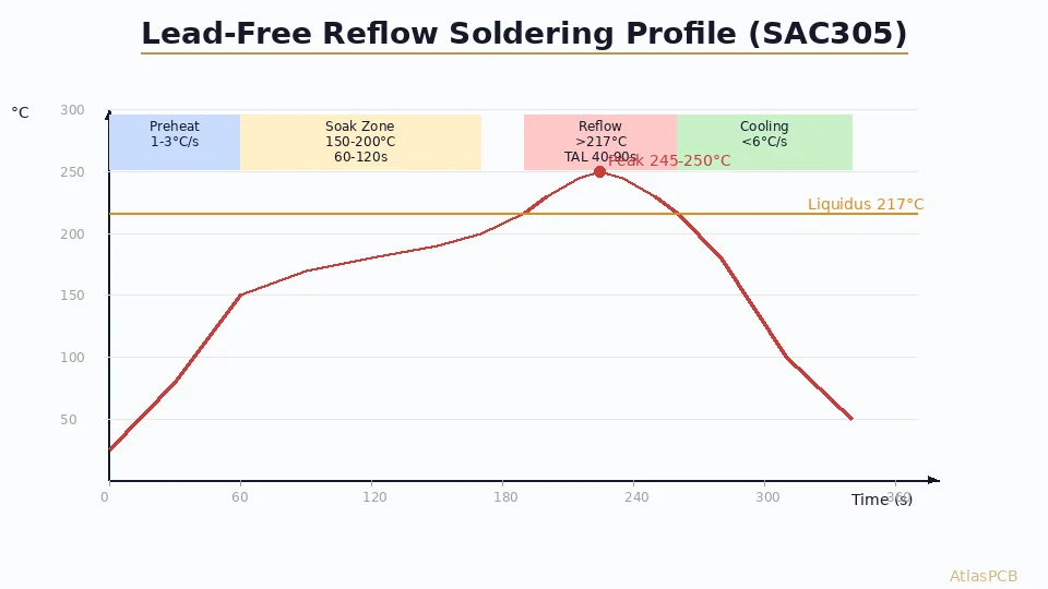
Step 3: Reflow Soldering
The board passes through a reflow oven where controlled heat melts the solder paste and forms permanent solder joints.
Reflow Profile Zones
- Preheat (25°C → 150°C): Gradual ramp at 1-3°C/second. Activates flux and drives off solvents.
- Soak/Thermal soak (150°C → 200°C): 60-120 seconds at near-constant temperature. Equalizes temperature across the board.
- Reflow (peak 235-250°C): Solder melts and wets the pads. Time above liquidus: 30-90 seconds.
- Cooling (250°C → 25°C): Controlled cooling at 2-4°C/second. Forms strong crystalline solder joints.
Lead-Free vs Leaded
| Parameter | SnPb (Leaded) | SAC305 (Lead-Free) |
|---|---|---|
| Melting point | 183°C | 217°C |
| Peak temp | 220-235°C | 240-250°C |
| Time above liquidus | 45-75s | 30-60s |
| Wetting | Excellent | Good |

Step 4: Through-Hole Assembly (If Required)
For boards with through-hole components (connectors, transformers, large capacitors):
Wave Soldering
- Flux application (spray or foam fluxer)
- Preheat (100-130°C)
- Board bottom passes over a wave of molten solder (250-260°C)
- Solder wicks up through the holes and forms joints
Selective Soldering
- Programmable solder nozzle applies solder only to specific through-hole joints
- Avoids disturbing previously soldered SMD components on the bottom side
- Slower but more precise than wave soldering
- Preferred for mixed-technology boards
Step 5: Inspection
AOI (Automated Optical Inspection)
- High-resolution cameras photograph every component and solder joint
- Software compares against programmed references
- Catches: missing parts, wrong orientation, misalignment, solder bridges, insufficient solder
- Placed after reflow and/or after wave soldering
X-Ray Inspection
- Required for BGA, QFN, and other bottom-terminated components
- Reveals: solder ball voiding, bridging, head-in-pillow defects
- 2D X-ray for screening, 3D CT for detailed analysis
Manual Visual Inspection
- Trained inspectors check areas AOI can’t reach
- Final visual quality check before packaging
- Uses magnification (10-40x) and good lighting
Step 6: Testing
ICT (In-Circuit Test)
- Bed-of-nails fixture tests component values and connections
- Catches: wrong values, missing components, opens, shorts
- Speed: 10-30 seconds per board
Functional Test (FCT)
- Board is powered and tested for correct operation
- Verifies: power rails, communication interfaces, sensor readings, LED indicators
- Custom test software and hardware for each product
Programming
- Microcontrollers and FPGAs are programmed via JTAG, SWD, UART, or custom interfaces
- Can be done during FCT or as a separate step
- Production programming typically uses gang programmers for speed
Step 7: Conformal Coating (Optional)
For products operating in harsh environments:
- Acrylic, silicone, urethane, or parylene coating applied to protect against moisture, dust, chemicals
- Applied by spray, dip, or selective coating robot
- Typical thickness: 25-75um
Step 8: Final Assembly and Packaging
- Depanelization (V-score breaking or router)
- Visual inspection of finished boards
- ESD-safe packaging (anti-static bags, foam)
- Labeling (serial numbers, date codes, compliance marks)
- Vacuum sealing with desiccant for moisture-sensitive products
PCBA Turnaround Times
| Service Level | Typical Lead Time |
|---|---|
| Quick-turn prototype | 24-72 hours |
| Standard prototype | 5-7 business days |
| Production (small batch) | 2-3 weeks |
| Production (mass) | 3-5 weeks |
Conclusion
PCBA is a precise, multi-step process where quality at each stage determines the reliability of the final product. Understanding the process helps designers create assembly-friendly layouts (DFA), specify appropriate quality levels, and communicate effectively with their assembly partner. Whether you need a 5-piece prototype or 100,000-unit production run, the fundamental process steps remain the same — only the level of automation and testing scales with volume.
Further Reading
[PCB Manufacturing Process: 15 Steps from Gerber to Finished Board]/blog/pcb-manufacturing-process-15-steps/)
[IPC Class 3 Requirements: The Complete Guide for Designers]/blog/ipc-class-3-requirements/)
About AtlasPCB — We specialize in complex PCB manufacturing for HDI, RF, and high-reliability applications. Explore our PCB assembly services . Every order includes free engineering review. Get your quote.
Reviewed by AtlasPCB Engineering Team — IPC-certified manufacturing specialists with 15+ years of production experience in HDI, RF, and high-reliability PCB fabrication. Content based on factory floor data and real customer design reviews.
- pcb assembly
- PCBA
- reflow soldering
- pick and place