· AtlasPCB Engineering · Engineering · 8 min read
PCB Layer-to-Layer Registration: Alignment Accuracy, Tolerances, and Manufacturing Methods
Complete guide to PCB layer-to-layer registration accuracy. Covers IPC Class 2 and Class 3 alignment tolerances, pin lamination vs mass lamination, X-ray registration systems, and design rules for achieving ±1 mil accuracy in HDI multilayer boards.

What Is Layer-to-Layer Registration?
Layer-to-layer registration refers to the positional accuracy with which copper patterns on different layers of a multilayer PCB align relative to each other and to drilled through-holes. In a perfectly registered board, all layer features align exactly as designed. In practice, manufacturing variations introduce offsets that must be controlled within specified tolerances.
Registration accuracy directly impacts:
- Annular ring integrity: Misaligned layers cause drill breakout, reducing pad-to-hole contact
- Controlled impedance: Lateral trace shift relative to reference planes alters characteristic impedance
- Signal integrity: Differential pair symmetry degrades when layers shift asymmetrically
- Reliability: Reduced annular rings fail earlier under thermal cycling stress
- BGA fanout: Tight-pitch BGA routing relies on precise via-to-pad alignment
For modern designs running PCIe Gen5/6, DDR5, or 56G+ SerDes, registration tolerance is as critical as trace width control.
IPC Registration Standards and Requirements
IPC-6012 Registration Classes
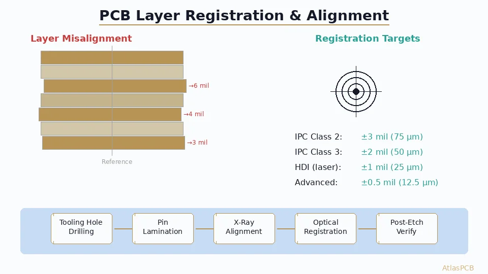
The IPC-6012 standard defines minimum registration requirements based on product class:
Class 2 — Standard Commercial Electronics
- Layer-to-layer registration: ±3 mil (75 μm)
- Layer-to-drill registration: ±4 mil (100 μm)
- Suitable for consumer electronics, IoT devices, general-purpose boards
Class 3 — High Reliability
- Layer-to-layer registration: ±2 mil (50 μm)
- Layer-to-drill registration: ±3 mil (75 μm)
- Required for telecom, industrial, automotive, medical devices
Class 3/A — Aerospace/Military
- Layer-to-layer registration: ±1.5 mil (38 μm)
- Layer-to-drill registration: ±2 mil (50 μm)
- Space, defense, and life-critical applications
Advanced HDI (Beyond IPC Standard)
- Layer-to-layer registration: ±1.0 mil (25 μm)
- Laser via to pad: ±0.5 mil (12.5 μm)
- Semiconductor packaging substrates: ±0.3 mil (8 μm)
How Registration Tolerance Affects Design Rules
The relationship between registration tolerance and minimum feature sizes:
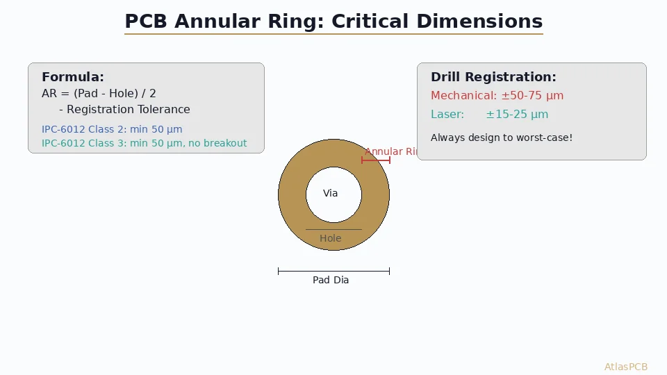
Minimum Annular Ring = (Pad Diameter - Drill Diameter) / 2 - Registration Tolerance
For example, with an 18 mil pad and 10 mil drill:
- Available annular ring = (18 - 10) / 2 = 4 mil
- Class 2 registration (±3 mil) → Effective minimum = 4 - 3 = 1 mil ⚠️ (barely acceptable)
- Class 3 registration (±2 mil) → Effective minimum = 4 - 2 = 2 mil ✓
This calculation demonstrates why tight-pitch designs often require Class 3 registration even for commercial products.
Manufacturing Methods for Registration Control
Pin Lamination (Standard Method)
Pin lamination is the most widely used registration method for multilayer PCBs:
- Tooling hole drilling: Precision holes drilled in each inner layer panel at fixed locations
- Pin alignment: Layers stacked on precision steel pins that pass through tooling holes
- Lamination press: Stack pressed under heat and pressure while pins maintain alignment
- Post-lamination drilling: Through-holes drilled using the same tooling hole reference
Achievable accuracy: ±2 to ±3 mil (50-75 μm)
Limitations:
- Tooling hole quality limits accuracy
- Material shrinkage during lamination introduces systematic offset
- Thermal expansion of pins during hot press cycle
- Panel warpage can cause local misalignment
Mass Lamination (High-Volume)
Used in high-volume Asian factories for standard consumer electronics:
- Slot/notch alignment: Layers indexed using edge slots rather than pins
- Optical pre-alignment: Camera systems verify alignment before press
- Rapid press cycle: High-throughput but slightly lower precision
Achievable accuracy: ±3 to ±4 mil (75-100 μm)
X-Ray Registration (High-Accuracy)
For HDI and high layer count boards, X-ray registration provides superior accuracy:
- X-ray targets: Special registration marks embedded in inner layers (copper targets)
- X-ray imaging: After lamination, X-ray system images internal targets through the panel
- Drill compensation: CNC drill program automatically compensates for measured offset
- Layer-specific correction: Each layer pair’s offset calculated independently
Achievable accuracy: ±1 to ±1.5 mil (25-38 μm)
Advantages:
- Compensates for post-lamination material movement
- Eliminates tooling hole dependency
- Enables independent correction for each drill span
- Required for 16+ layer builds and any-layer HDI
Laser Direct Imaging (LDI) with Registration
Modern LDI exposure systems can incorporate real-time registration compensation:
- Fiducial reading: Camera reads panel fiducials before exposure
- Image scaling: Digital artwork scaled to match actual panel dimensions
- Local correction: Different areas of the panel receive independent scaling
- Compensation data: Feed-forward from previous process steps
This approach addresses the material dimensional changes that occur during processing rather than just managing mechanical alignment.
Sources of Registration Error
Material Dimensional Instability
FR-4 base material changes dimensions during processing:
- After copper etching: Stress relief causes 0.02-0.05% shrinkage
- During oxide/alternative oxide: Thermal cycle causes 0.01-0.03% expansion
- During lamination: Compression and heat cause complex dimensional changes
- After reflow: Additional 0.01% dimensional change possible
For a 500 mm panel, a 0.03% dimensional change equals 150 μm (6 mil) — significant for registration.
Copper Pattern Influence
Non-uniform copper distribution causes anisotropic dimensional changes:
- Heavy copper areas resist material movement
- Sparse copper areas allow more shrinkage
- This creates localized registration shift (sometimes called “artwork shift”)
- Copper balancing helps maintain uniform dimensional stability
Process-Induced Errors
| Error Source | Typical Magnitude | Mitigation |
|---|---|---|
| Tooling hole accuracy | ±0.5 mil | Precision CNC drilling |
| Pin diameter tolerance | ±0.1 mil | Ground steel pins, regular calibration |
| Material shrinkage | 0.02-0.05% | Scaling compensation artwork |
| Thermal expansion (press) | Variable | Controlled ramp rates |
| Sequential lamination (per cycle) | +0.3-0.5 mil | X-ray registration |
| LDI exposure accuracy | ±0.3 mil | Regular calibration |
Tight Registration Requirements for Your HDI Design?
AtlasPCB achieves ±1 mil layer registration with X-ray alignment systems. We provide registration coupons on every panel for verification.
Request HDI Capabilities Review →Design for Registration: DFM Guidelines
Annular Ring Sizing Strategy
Design annular rings to accommodate worst-case registration:
Start with minimum copper annular ring required by IPC class
- Class 2: 2 mil minimum (external), 1 mil (internal)
- Class 3: 3 mil minimum (external), 2 mil (internal)
Add registration tolerance margin
- Add full registration tolerance value for a 100% yield target
- Add 75% for a practical ~99.7% yield target (3σ process)
Consider drill accuracy separately
- Mechanical drill: ±2 mil position accuracy
- Laser drill: ±0.5 mil position accuracy
- Total positional tolerance = √(registration² + drill²) for RSS method
Registration-Friendly Design Practices
Artwork Scaling Compensation
- Work with your fabricator to determine their standard scaling factors
- Typical inner layer artwork is scaled 1.0002-1.0005× to pre-compensate for shrinkage
- Some fabricators use predictive models based on copper density
Fiducial and Target Placement
- Place registration targets in panel frame area (4 corners minimum)
- Add targets within board outline for large boards (>300 mm)
- Use copper-cleared circular targets (1-2 mm diameter) visible to optical systems
Layer Pair Optimization
- Keep critical signal-reference pairs on the same core (laminated together)
- Avoid routing critical differential pairs on layers that span multiple sequential laminations
- Place highest-density BGA breakout on layers closest to the same core
Via Design for Registration Tolerance
For through-hole vias in Class 3 designs:
| Via Drill | Minimum Pad | Annular Ring (after plating) | Registration Budget |
|---|---|---|---|
| 8 mil | 16 mil | 4 mil | ±2 mil Class 3 |
| 10 mil | 18 mil | 4 mil | ±2 mil Class 3 |
| 12 mil | 20 mil | 4 mil | ±2 mil Class 3 |
| 6 mil (laser) | 10 mil | 2 mil | ±1 mil HDI |
Verification and Measurement
Registration Coupon Design
Include dedicated registration measurement coupons in the panel frame:
- Type 1 — Layer-to-layer: Targets on each layer pair measured by X-ray or cross-section
- Type 2 — Layer-to-drill: Targets around drilled holes measured by optical inspection
- Type 3 — Full registration map: Grid of targets across the panel for spatial uniformity data
Measurement Methods
- Microsection: Cross-section and measure under microscope (destructive, highest accuracy)
- X-ray inspection: Non-destructive measurement of internal target alignment
- Electrical test: Dedicated registration coupon with breakable connections at tolerance limits
- Automated optical inspection (AOI): Surface layer-to-drill registration check
Statistical Process Control
Leading fabricators track registration data in SPC charts:
- Cpk ≥ 1.33 indicates process capability meeting spec with margin
- Regular Gauge R&R studies validate measurement system
- Trend analysis predicts when tooling/calibration maintenance is needed
Impact on High-Speed Signal Integrity
Registration errors affect signal integrity in several ways:
Impedance Variation
A trace designed for 50Ω impedance on a 4 mil dielectric will see impedance shift if registration moves the trace laterally relative to its reference plane:
- 1 mil lateral shift: ~1-2% impedance change
- 2 mil lateral shift: ~3-5% impedance change
- 3 mil lateral shift: ~5-8% impedance change
Differential Pair Skew
When the signal layer registration differs from the reference plane registration, one trace of a differential pair may be closer to the reference plane than the other, creating:
- Propagation velocity imbalance
- Common-mode noise generation
- Effective skew equivalent to 1-3 ps per mil of registration error
Pad-to-Anti-pad Clearance
Via anti-pads (clearance holes in planes) must maintain adequate clearance even with registration error. If the via shifts but the anti-pad doesn’t (or vice versa), the plane copper encroaches on the barrel, creating capacitive loading or, in worst cases, a short circuit.
Related Design Considerations
- Annular ring standards: How registration tolerance feeds into pad sizing
- HDI stackup design: Sequential lamination and registration challenges
- Controlled impedance design: How alignment affects impedance control
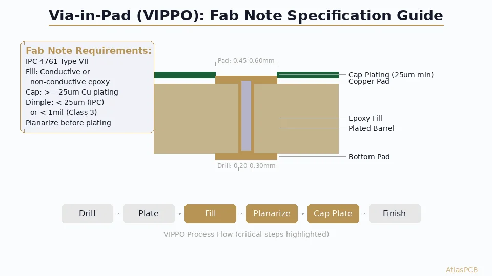
- Via-in-pad design: Registration requirements for VIPPO processes
Conclusion
Layer-to-layer registration is a foundational capability that constrains minimum feature sizes, determines pad geometries, and influences signal integrity margins. By understanding the registration capabilities of your chosen fabrication process — and designing with appropriate margins — you avoid yield-limiting annular ring violations and maintain the electrical performance your design requires.
For HDI and high layer count designs targeting ±1 mil registration, specify X-ray alignment in your fabrication notes and include registration measurement coupons. Work with fabricators who provide Cpk data demonstrating their registration process capability matches your design needs.
Designing a board with tight registration requirements? AtlasPCB’s HDI and multilayer capabilities include X-ray registration alignment systems achieving ±1 mil accuracy. We include registration coupon data in our quality reports. Upload your design for review →
About AtlasPCB — We specialize in complex PCB manufacturing for HDI, RF, and high-reliability applications. Explore our HDI PCB manufacturing capabilities, multilayer PCB fabrication up to 30 layers, or get an free engineering DFM review . Every order includes free engineering review. Get your quote.
Reviewed by AtlasPCB Engineering Team — IPC-certified manufacturing specialists with 15+ years of production experience in HDI, RF, and high-reliability PCB fabrication. Content based on factory floor data and real customer design reviews.
- layer registration
- PCB alignment
- multilayer PCB
- IPC tolerances
- HDI
- pin lamination
- X-ray alignment
- annular ring
- DFM
- manufacturing process