· AtlasPCB Engineering · Engineering · 10 min read
How to Specify Impedance-Controlled PCB Stackup: Complete Ordering Checklist
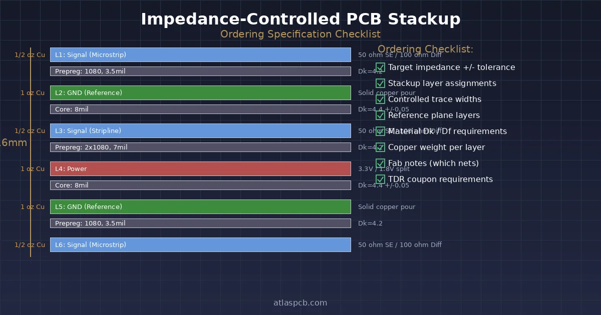
The 8-Item Checklist: What Your Fab Needs From You
Before submitting your impedance-controlled design, confirm you have these eight items ready:
- Target impedance values — Single-ended (typically 50 ohm) and/or differential (typically 90 or 100 ohm), with tolerance (+/-10% or +/-5%)
- Stackup drawing — Layer order, copper weights, dielectric thicknesses, material callout
- Impedance table — Which layers, which trace widths, which reference planes, SE or differential
- Dielectric material preference — Standard FR-4, High-Tg FR-4, Isola 370HR, Megtron, or “fab choice within Dk range”
- Controlled trace widths in your Gerber — The widths you designed for, based on your field solver results
- Reference plane assignments — Which copper layer is the return path for each signal layer
- Fab notes — Clear text in your README or drawing specifying impedance requirements
- Permission to adjust — Explicitly state whether the fab may modify trace widths (+/-0.5-1.5mil) to hit impedance targets
Missing any of these will trigger an engineering query from your fab, adding 1-3 days to your lead time.
IMPEDANCE CONTROL
Free Stackup Review Before You Order
Upload your stackup and impedance requirements. Our SI engineers will verify with Polar field solver and confirm manufacturability before production.
Submit for Review ›What “Impedance Controlled” Actually Means in Manufacturing
When you mark a board as impedance-controlled, you are telling the fab that certain traces must have a characteristic impedance within a specified tolerance when measured by TDR. This is not the same as simply following your Gerber files exactly.
The fab commits to:
- Using calibrated dielectric materials with known Dk at your operating frequency
- Controlling etch processes to hold trace widths within +/-0.5mil of target
- Controlling lamination to hit dielectric thickness within +/-10% (or tighter for premium)
- Building TDR test coupons on the panel border that replicate your controlled trace geometry
- Measuring every production panel and providing a TDR report (if requested)
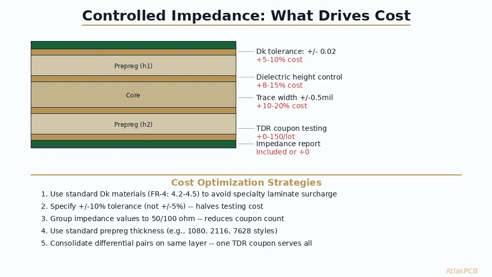
Standard tolerance: +/-10% means a 50-ohm target will measure between 45 and 55 ohms on the test coupon. This is achievable with standard FR-4 and normal process controls.
Premium tolerance: +/-5% means a 50-ohm target must measure between 47.5 and 52.5 ohms. This typically requires:
- Controlled-Dk material (Dk variation < +/-2% lot-to-lot)
- Tighter etch control (trace width tolerance +/-0.3mil)
- More expensive prepreg grades with consistent resin content
- Price premium of 10-20%
Required Documentation: What Goes in Your Package
Stackup Drawing
Your stackup drawing must include:
- Layer names matching your Gerber file names (L1, L2… or Top, GND, PWR, Signal, Bot)
- Copper weight for each layer (0.5oz, 1oz, 2oz)
- Dielectric thickness between each copper layer (in mils or mm)
- Material type (FR-4, High-Tg, specific laminate like 370HR)
- Total board thickness target and tolerance
- Which layers are signal, ground, or power
Example of a clear stackup callout:
L1  (Signal)   - 1oz Cu - Outer
    Prepreg    - 4.5mil (1080, Dk 4.2 @ 1GHz)
L2  (Ground)   - 0.5oz Cu - Inner
    Core       - 8.0mil (Dk 4.4 @ 1GHz)
L3  (Signal)   - 0.5oz Cu - Inner
    Prepreg    - 4.5mil (1080, Dk 4.2 @ 1GHz)
L4  (Power)    - 0.5oz Cu - Inner
    Core       - 8.0mil (Dk 4.4 @ 1GHz)
L5  (Signal)   - 0.5oz Cu - Inner
    Prepreg    - 4.5mil (1080, Dk 4.2 @ 1GHz)
L6  (Ground)   - 0.5oz Cu - Inner
    Core       - 8.0mil (Dk 4.4 @ 1GHz)
L7  (Signal)   - 0.5oz Cu - Inner
    Prepreg    - 4.5mil (1080, Dk 4.2 @ 1GHz)
L8  (Signal)   - 1oz Cu - Outer
    Total: ~62mil (1.6mm)
Impedance Table
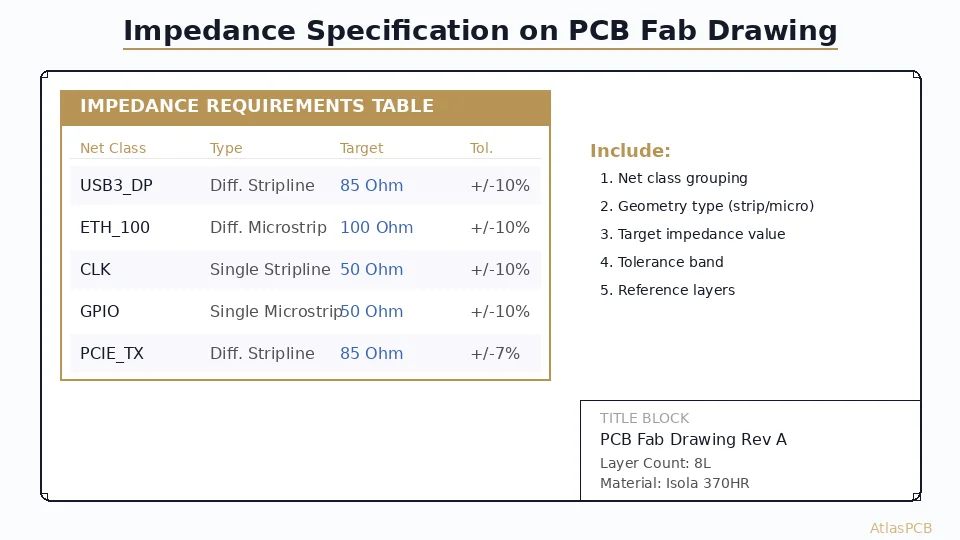
Present your impedance requirements in a simple table format in your fab notes or README:
| Layer | Type | Width (mil) | Space (mil) | Reference | Target (ohm) | Tolerance |
|---|---|---|---|---|---|---|
| L1 | Single-ended | 4.0 | — | L2 (GND) | 50 | +/-10% |
| L1 | Differential | 4.0 | 5.0 | L2 (GND) | 100 | +/-10% |
| L3 | Single-ended | 3.8 | — | L2 (GND) | 50 | +/-10% |
| L7 | Differential | 3.8 | 5.0 | L6 (GND) | 90 | +/-10% |
Common Mistakes That Cause Delays
These are the top five errors we see in impedance-controlled orders, ranked by frequency:
1. Missing Dielectric Constant Specification
Saying “FR-4” without specifying Dk is like ordering “steel” without specifying the alloy. Standard FR-4 Dk ranges from 4.0 to 4.8 depending on glass style (1080, 2116, 7628) and resin content (50-65%). If your field solver assumed Dk = 4.2 but the fab uses a prepreg with Dk = 4.6, your impedance will be off by ~5%.
Fix: Either specify the exact prepreg (e.g., “1080 prepreg, 53% RC, Dk 4.2 at 1 GHz”) or state “Fab to select material to achieve target impedance” and let the fab’s field solver drive material choice.
2. Wrong Reference Plane Assignment
A 4.0mil trace referenced to a ground plane 4.5mil away gives ~50 ohms. The same trace referenced to a ground plane 8.0mil away gives ~70 ohms. If your impedance table says “Layer 1 referenced to Layer 2” but Layer 2 is actually power (with splits and voids), the impedance will be uncontrolled in areas where the reference plane is absent.
Fix: Always reference to a continuous ground plane. If you must reference to a power plane, ensure it is unbroken beneath all controlled traces.
3. Inconsistent Units
Mixing mils and millimeters in the same document, or specifying trace width in mils but dielectric in millimeters, causes confusion and potential errors.
Fix: Pick one unit system and use it consistently. Mils (thousandths of an inch) is the PCB industry standard in most Western fabs.
4. Not Accounting for Etch Factor
Outer layers lose copper during etching (trapezoidal cross-section). A trace designed at 4.0mil on an outer layer with 1oz copper will etch to approximately 3.2-3.5mil at the base due to undercut. Your fab compensates for this, but if you have already compensated in your Gerber, you get double compensation.
Fix: Design to your target trace width. State in fab notes that the fab should compensate for etch factor. Do not pre-compensate unless you explicitly communicate this.
5. Requesting Impedance Control on Every Net
Marking all signal nets as impedance-controlled forces the fab to treat the entire board as a controlled product, increasing cost and scrutiny on traces that do not need it (GPIO, I2C at 400kHz, reset lines).
Fix: Only flag nets that actually require impedance control: high-speed serial links, DDR data/address buses, RF traces, USB, Ethernet, PCIe, HDMI.
ENGINEERING SUPPORT
Unsure About Your Stackup?
Our engineers run Polar SI9000 simulations on your stackup for free during quoting. No NRE charge for impedance modeling.
Request Stackup Simulation ›Material Selection: Impact on Impedance Tolerance
The dielectric constant (Dk) of your laminate material directly determines achievable impedance tolerance. Here is how common materials compare:
| Material | Dk @ 1 GHz | Dk Tolerance (lot-to-lot) | Best For |
|---|---|---|---|
| Standard FR-4 (generic) | 4.2-4.8 | +/-5-8% | General, <3 GHz |
| Isola 370HR (High-Tg) | 4.04 | +/-3% | Controlled impedance, lead-free |
| Isola I-Speed | 3.63 | +/-2% | 5-15 GHz, tight impedance |
| Panasonic Megtron 6 | 3.40 | +/-1.5% | 10+ GHz, premium SI |
| Rogers RO4350B | 3.48 | +/-1.5% | RF, microwave, antenna |
Key insight: If your impedance tolerance budget is +/-10%, standard FR-4 works fine because the fab adjusts trace widths based on actual measured Dk of the incoming material lot. The fab’s field solver uses the real Dk, not the datasheet typical value.
If your tolerance budget is +/-5%, you need either:
- A controlled-Dk material (Dk variation < +/-2%), OR
- A fab willing to sort prepreg lots and use only matching Dk batches (adds cost and lead time)
How to Write Effective Fab Notes
Your fab notes are the single most important communication channel for impedance-controlled boards. Here is a template:
IMPEDANCE CONTROL REQUIREMENTS:
- Board is impedance-controlled per table below
- Fab may adjust trace widths +/-1.0mil to meet impedance targets
- Tolerance: +/-10% unless noted otherwise
- TDR test coupon required on panel border
- Please provide TDR report with shipment

IMPEDANCE TABLE:
Layer 1 (Top):  50 ohm SE, 4.0mil trace, ref to L2 (GND)
Layer 1 (Top): 100 ohm diff, 4.0/5.0mil W/S, ref to L2 (GND)
Layer 3 (Sig):  50 ohm SE, 3.8mil trace, ref to L2 (GND)
Layer 6 (Sig): 100 ohm diff, 3.8/5.0mil W/S, ref to L7 (GND)

MATERIAL:
- High-Tg FR-4 (Tg >= 170C), Dk 4.0-4.4 at 1GHz acceptable
- Fab to select prepreg glass style to achieve impedance targets
- Total thickness: 1.6mm +/-10%
What NOT to Put in Fab Notes
- Do not specify an exact prepreg Dk (like “Dk must be exactly 4.2”) unless you are willing to pay for sorted material lots
- Do not over-constrain by specifying both exact dielectric thickness AND exact impedance — let the fab optimize one to achieve the other
- Do not reference your EDA tool’s stackup simulation without providing the actual numbers — the fab does not have your Altium/KiCad project file
Verification: How Impedance Is Tested
After fabrication, the fab measures impedance using TDR (Time Domain Reflectometry) on test coupons. Understanding this process helps you design better:
- Coupons are built on panel borders with traces that exactly mirror your controlled signal traces (same width, same layer, same dielectric)
- TDR sends a fast pulse through the coupon trace and measures the reflection to calculate impedance along the trace length
- Each panel is tested — if coupons fail, the entire panel is scrapped
- Reports show measured impedance vs. target, with pass/fail per coupon
You can request:
- Standard: TDR coupon test, pass/fail noted on lot traveler
- Enhanced: TDR report included with shipment (PDF with measured values)
- Premium: 100% panel TDR with statistical data (Cpk reporting)
SIGNAL INTEGRITY
Impedance-Controlled Boards From 5 Days
Standard +/-10% tolerance with TDR report included at no extra charge. Premium +/-5% available for high-speed designs.
Get Quote With TDR Report ›Communicating Changes Mid-Order
If the fab’s field solver shows your target impedance is not achievable with your specified stackup, they will issue an Engineering Query (EQ). Typical EQ scenarios:
- “Your 4.0mil trace on L1 with 4.5mil prepreg gives 47.2 ohm, not 50. Can we widen to 4.3mil?”
- “The 2116 prepreg available gives Dk 4.5 instead of the 4.2 you specified. Can we thin the prepreg to 3.8mil to compensate?”
- “Your differential pair at 3.5/4.0mil W/S gives 105 ohm, not 100. Can we reduce spacing to 3.5mil?”
Best practice: Pre-authorize trace width adjustments in your fab notes (the ”+/-1.0mil” permission mentioned above). This eliminates most EQs and can save 1-2 days on your lead time.
Summary: Quick Reference
| If You Want… | You Need To… |
|---|---|
| +/-10% impedance | Standard FR-4 + clear fab notes + impedance table |
| +/-5% impedance | Controlled-Dk material + specify material grade + accept 10-20% cost increase |
| TDR report | Request it explicitly in fab notes |
| Fastest turnaround | Pre-authorize trace width adjustments + provide complete documentation |
| Lowest cost | Use standard FR-4 + +/-10% tolerance + let fab choose prepreg |
ATLASPCB
Order Impedance-Controlled PCBs With Confidence
Upload your Gerber + stackup. Our engineers verify impedance feasibility before production starts. No surprises, no delays.
Start Your Order ›Related Reading
- PCB Capabilities and Specifications — Full list of supported materials, layer counts, and tolerances
- Rigid PCB Manufacturing Services — Standard rigid board production including impedance control
- Signal Integrity Starts With Stackup Design — Deeper dive into stackup planning for high-speed designs
About AtlasPCB — We specialize in complex PCB manufacturing for HDI, RF, and high-reliability applications. Explore our impedance-controlled PCB manufacturing, or get an free engineering DFM review . Every order includes free engineering review. Get your quote.
Reviewed by AtlasPCB Engineering Team — IPC-certified manufacturing specialists with 15+ years of production experience in HDI, RF, and high-reliability PCB fabrication. Content based on factory floor data and real customer design reviews.
- impedance control
- stackup design
- signal integrity
- DFM
- ordering guide