· Engineering · 8 min read
PCB Thermal Design for Edge AI Inference Modules: Copper Pour Strategy and Via Array Optimization
Practical thermal management guide for PCBs carrying edge AI inference modules (NVIDIA Jetson, Hailo-8, Google Coral). Covers thermal via array sizing, copper pour techniques, stackup considerations, and heat spreader integration for processors dissipating 5-25W in compact form factors.
Quick Design Parameters
| Parameter | Recommendation | Notes |
|---|---|---|
| Thermal via diameter | 0.3mm (filled) or 0.25mm (tented) | Filled preferred |
| Via pitch | 0.6-0.8mm | Tighter = better, limited by drill registration |
| Minimum via count | 25 (5x5 array) for 10W module | Scale linearly with power |
| Copper weight (outer) | 2oz (70um) minimum | 3oz for >20W |
| Copper weight (inner) | 1oz (35um) minimum | 2oz if budget allows |
| Minimum ground planes | 2 continuous planes | More planes = more spreading |
| Exposed pad solder paste | 50-60% coverage pattern | Prevents voiding while maintaining thermal contact |
| PCB thickness | 1.6mm standard | Thinner = lower thermal resistance through via |
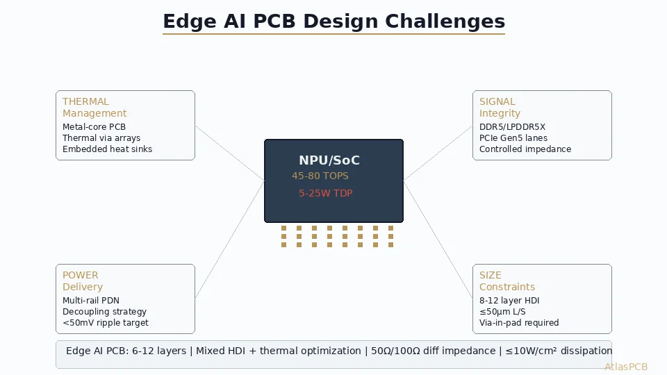
The Thermal Challenge: Edge AI in Compact Form Factors
Edge AI inference modules present a specific thermal problem: high power density (5-25W) in small packages (15x15mm to 30x30mm), mounted on compact PCBs (often 50x80mm or smaller), frequently in sealed enclosures without active cooling.
Unlike server-class AI accelerators where liquid cooling and massive heatsinks are standard, edge AI boards must dissipate heat through the PCB itself and a modest heatsink. The PCB becomes a critical thermal component, not just an electrical interconnect.
Typical edge AI modules and their thermal profiles:
| Module | TDP | Package Size | Exposed Pad |
|---|---|---|---|
| NVIDIA Jetson Orin Nano | 7-15W | 29.9x29.9mm (SoM) | Yes, bottom |
| Hailo-8 | 2.5W (typical), 5W (peak) | 13x13mm BGA | 9x9mm exposed |
| Google Coral Edge TPU | 2-4W | 10x10mm | 6x6mm exposed |
| Intel Movidius Myriad X | 1-2W | 12x12mm | No exposed pad |
| Custom FPGA inference (Xilinx KV26) | 10-25W | 23x23mm | 16x16mm exposed |
The heavier designs (Jetson, FPGA-based) absolutely require optimized PCB thermal paths. Even the lighter modules (Hailo, Coral) benefit from proper thermal design in sealed enclosures where ambient rises to 50-60C.
AI HARDWARE PCB DESIGN
Building an Edge AI Product?
AtlasPCB fabricates boards for AI inference hardware with optimized thermal stackups — 2-3oz copper, conductive-filled thermal vias, and metal-core options for high-dissipation modules.
Get AI Board Quote ›Thermal Via Array Design: Sizing and Layout
Step 1: Determine Required Thermal Resistance
For reliable operation, the total thermal resistance from junction to ambient must keep Tj below the module’s maximum (typically 105-125C for commercial-grade AI chips):
Tj = Ta + P * (Rjc + Rpcb + Rhs)

Where:
- Ta = ambient temperature (design for worst case: 50-60C in enclosure)
- P = module TDP (watts)
- Rjc = junction-to-case thermal resistance (from datasheet)
- Rpcb = PCB thermal resistance (what you're designing)
- Rhs = heatsink-to-ambient (if used)
Target: Rpcb < 15 C/W for modules up to 15W. Below 10 C/W for 20W+ modules.
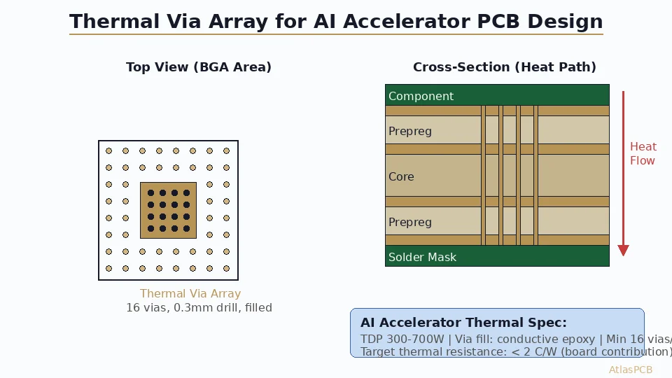
Step 2: Size the Via Array
Each filled thermal via (0.3mm drill, 25um plating, 1.6mm board) provides approximately:
- Plated through-hole (unfilled): Rvia ~ 70-100 C/W per via
- Non-conductive filled + capped: Rvia ~ 50-70 C/W per via
- Conductive filled (copper epoxy): Rvia ~ 20-40 C/W per via
Vias in parallel: Rtotal = Rvia / N (where N = number of vias)
Example calculation for 15W Jetson Orin Nano:
- Target Rpcb = 12 C/W
- Using conductive-filled vias (Rvia ~ 30 C/W each)
- Required vias: 30/12 = 2.5 → minimum 3 vias (but practically, use 25-36 for uniform heat distribution)
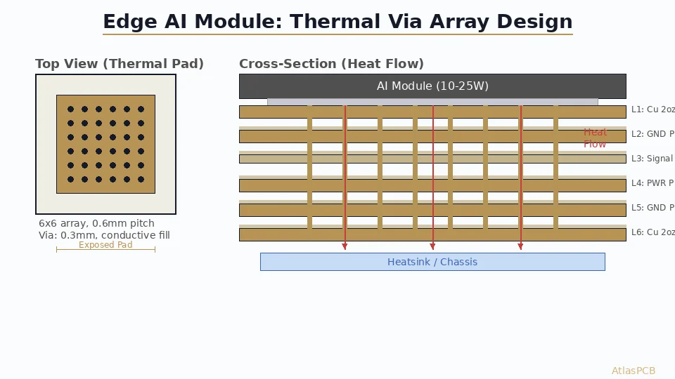
- A 6x6 array (36 vias) on 0.6mm pitch fits within a 3.6x3.6mm area — well within the exposed pad footprint
Step 3: Via Layout Rules
- Pitch: 0.6mm minimum (limited by drill-to-drill clearance). 0.8mm more conservative.
- Edge clearance: Keep vias 0.3mm inward from exposed pad edge
- Solder paste pattern: Use windowed stencil (50-60% coverage) over thermal pad to prevent solder voiding
- Via fill requirement: Mandatory for pads that will be soldered. Unfilled vias wick solder away from the joint.
- Avoid vias directly under BGA balls in the non-thermal area of the same component
Copper Pour Strategy for Lateral Heat Spreading
Thermal vias transfer heat vertically (Z-axis). Copper planes spread heat laterally (X-Y plane). Both are essential.
Inner Layer Copper Pour Rules
- Dedicate at least 2 inner layers as unbroken copper planes under the AI module footprint
- Minimum copper fill: 80% in the thermal zone (25mm radius from module center)
- Avoid routing signals through the thermal zone on ground/power planes — every trace cut reduces thermal spreading
- Connect thermal vias to ALL inner copper planes — each connected plane adds parallel thermal spreading area
- Extend copper planes beyond the module footprint — the spreading radius should be at least 2x the module dimension in each direction
Outer Layer Copper Strategy
- Bottom layer (opposite side from module): Maximum copper fill with thermal pad for heatsink attachment or convective cooling
- Top layer (module side): Copper fill around module perimeter. Keep ground flood connected to via array.
- Thermal relief: Do NOT use thermal reliefs on thermal via connections to planes. Use solid connections (direct connect) for minimum thermal resistance.
Critical design error: Using thermal relief pads on thermal vias. The spoke pattern adds 2-5 C/W per plane connection. For AI module thermal vias, always use solid (direct) pad-to-plane connections.
THERMAL STACKUP OPTIMIZATION
Heavy Copper for AI Thermal Management
Up to 5oz outer copper, 3oz inner copper. Conductive-filled thermal via arrays. Metal-core options for extreme dissipation. Boards up to 30 layers for complex AI SoC routing.
Discuss Your Thermal Design ›Stackup Considerations for Edge AI Boards
4-Layer Stackup (Budget Edge AI, < 10W)
L1: Signal + Component (2oz) — module on this side
L2: Ground plane (1oz) — continuous under module
L3: Power plane (1oz) — continuous under module
L4: Signal + Thermal pad (2oz) — heatsink attach side
Thermal path: Module → solder joint → thermal vias → L2/L3 planes (spreading) → L4 copper pad → heatsink/air
6-Layer Stackup (Performance Edge AI, 10-20W)
L1: Signal + Component (2oz)
L2: Ground plane (1oz) — thermal spreading
L3: Signal (1oz) — route AWAY from thermal zone
L4: Power plane (1oz) — thermal spreading
L5: Ground plane (1oz) — thermal spreading
L6: Signal + Thermal pad (2oz) — heatsink side
Three continuous copper planes (L2, L4, L5) provide excellent lateral spreading. Route high-speed signals on L3 but avoid the thermal zone directly under the module.
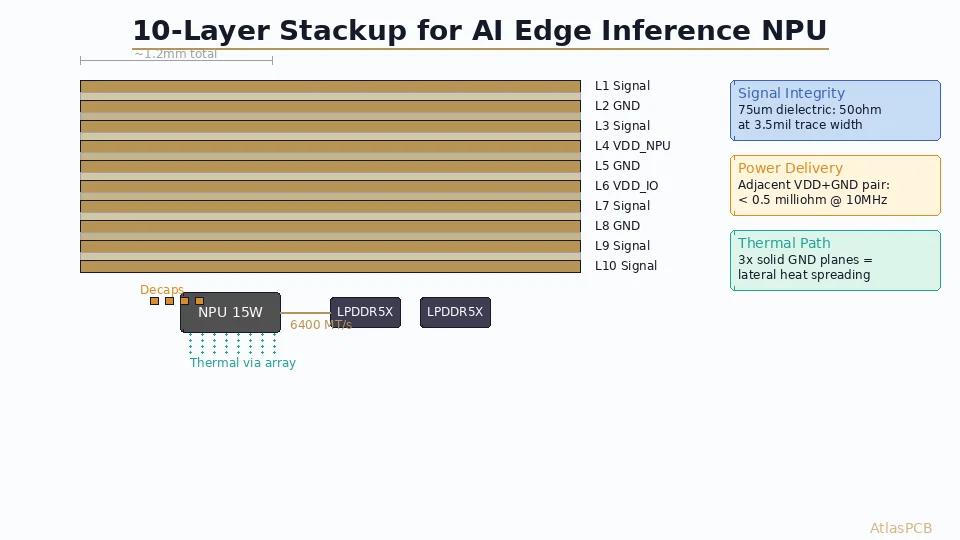
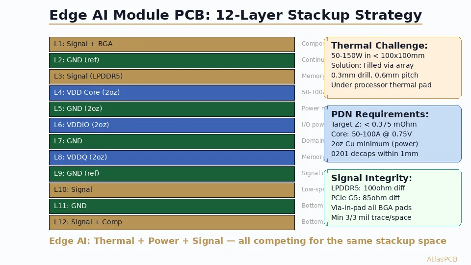
8-Layer Stackup (High-Performance AI SoC, 15-25W)
L1: Signal + Component (2oz)
L2: Ground (2oz) — primary thermal spreading
L3: Signal (1oz) — DDR/PCIe routing
L4: Power (1oz) — VRM planes
L5: Ground (1oz) — signal return/thermal
L6: Signal (1oz) — DDR/PCIe routing
L7: Power (1oz) — thermal spreading
L8: Signal + Thermal pad (2oz) — heatsink
For detailed stackup design methodology, see our guide on AI accelerator PCB thermal and power delivery design.
Heatsink Integration: PCB Interface Design
The PCB bottom layer (opposite the AI module) often interfaces with a chassis heatsink or heat spreader. Design considerations:
Thermal interface pad: Expose copper (no solder mask) in a defined area matching the heatsink contact footprint. Specify ENIG or immersion silver finish to prevent oxidation while maintaining thermal contact.
Flatness requirement: PCB warpage in the heatsink contact zone must be < 100um to ensure thermal interface material (TIM) fills the gap uniformly. For boards with heavy copper planes, specify < 0.5% bow/twist per IPC-6012.
Mounting hardware: Plan for heatsink mounting screws/clips in the PCB layout. Through-board mounting holes near the thermal zone help clamp the PCB flat against the heatsink.
EDGE AI HARDWARE
From ML Model to Production Hardware
Whether you're designing carrier boards for Jetson modules, custom inference accelerators, or AI-at-the-edge sensor fusion platforms — we fabricate the boards that make edge AI reliable.
Start Your AI Hardware Project ›Validation: How to Verify Your Thermal Design
Before committing to production, verify thermal performance:
Thermal simulation: Use Ansys Icepak or Siemens FloTHERM to model board-level thermal resistance. Input actual copper fill percentages, via array parameters, and enclosure conditions.
First-article thermal testing: Place thermocouples on module case (top) and PCB bottom (under via array). Run inference workload at maximum utilization for 30 minutes. Verify steady-state temperatures.
IR thermal imaging: Non-contact verification of heat spreading pattern. Reveals uneven thermal distribution caused by insufficient copper fill or broken ground planes.
Acceptance criteria:
- Tj < Tj_max - 20C margin (accounts for aging and manufacturing variation)
- PCB bottom temperature uniform within +/-5C across thermal zone
- No hotspots indicating void in thermal via fill
ATLASPCB
Thermal-Optimized PCBs for AI Hardware — Prototype in 7 Days
Heavy copper, conductive via fill, metal-core options. Up to 30 layers for complex AI SoC designs. Upload your Gerber files and get an instant quote with thermal stackup recommendations.
Get Instant Quote ›Related Reading:
About AtlasPCB — We specialize in complex PCB manufacturing for HDI, RF, and high-reliability applications. Explore our aluminum and metal-core PCB services . Every order includes free engineering review. Get your quote.
Reviewed by AtlasPCB Engineering Team — IPC-certified manufacturing specialists with 15+ years of production experience in HDI, RF, and high-reliability PCB fabrication. Content based on factory floor data and real customer design reviews.
- ai-hardware
- thermal-management
- edge-ai
- pcb-design
- copper-pour