· AtlasPCB Engineering · Engineering · 13 min read
CAF Resistance in PCBs: Conductive Anodic Filament Prevention and Design Rules
Comprehensive guide to Conductive Anodic Filament (CAF) formation in PCBs — the electrochemical migration mechanism along glass fibers, IPC-TM-650 test methods, design spacing rules, material selection strategies, and humidity effects on CAF resistance.
CAF Resistance in PCBs: Conductive Anodic Filament Prevention and Design Rules
Among the many reliability threats facing PCB assemblies, Conductive Anodic Filament (CAF) formation is one of the most insidious. Unlike a solder joint crack or a plating defect — failures you can find with standard inspection — CAF grows invisibly inside the laminate, along pathways you cannot see, until it creates a short circuit that may appear intermittent, inexplicable, and maddening.
CAF failures have brought down aerospace systems, caused field returns in automotive electronics, and plagued high-voltage industrial controllers. As PCB designs shrink conductor spacing, increase layer counts, and operate in harsher environments, understanding and preventing CAF has never been more important.
This article provides the definitive engineering reference for CAF: what it is, how it forms, how to test for it, and — most importantly — how to prevent it through material selection, design rules, and process control.
What Is Conductive Anodic Filament (CAF)?
CAF is a subsurface electrochemical migration phenomenon in which metallic copper grows as a filament along the interface between the glass fiber reinforcement and the epoxy resin matrix inside a PCB laminate. The filament originates at the anode (positive electrode) and propagates toward the cathode (negative electrode), eventually bridging the gap between two conductors and causing an electrical short.
The term “anodic” refers to the origin of the filament — it starts at the anode, where copper oxidizes and dissolves into the electrolyte (absorbed moisture). The dissolved copper ions migrate along the glass-resin interface, driven by the electric field, and are reduced back to metallic copper as they approach the cathode.
CAF vs. Other Electrochemical Migration (ECM) Types
CAF is one specific form of electrochemical migration. Other types include:
- Surface ECM (dendrites): Metal migration across the board surface, usually visible under magnification
- Conductive Filament Formation (CFF): General term that includes CAF and other subsurface migration
- Ionic contamination: Residual flux or processing chemicals creating conductive paths
What makes CAF uniquely dangerous is that it occurs inside the laminate — invisible to visual inspection, AOI, and even X-ray in early stages. It only becomes detectable when the insulation resistance drops to measurable levels, by which point the filament is well-established.
The Three Requirements for CAF Formation
CAF requires all three of the following conditions to exist simultaneously. Eliminating any one prevents CAF growth:
1. A Pathway: Fiber-Resin Interface Separation
The glass fibers in PCB laminates are coated with a silane coupling agent that bonds the glass to the epoxy resin. When this bond is intact, there is no pathway for migration. CAF can only grow where the glass-resin interface has separated (delaminated), creating a microscopic channel.
What causes fiber-resin separation?
- Thermal stress: Reflow soldering, rework, wave soldering — any process that heats the board above Tg causes differential expansion between glass and resin, stressing the interface
- Mechanical drilling: The drill bit creates microfractures at the intersection of drilled holes and glass fiber bundles. This is the most common CAF initiation site — between two PTH vias or between a PTH and an internal trace
- Moisture absorption: Water penetrates the glass-resin interface, weakening the bond through hydrolysis of the silane coupling agent
- Poor lamination: Insufficient resin flow during lamination leaves voids at the fiber-resin interface
- Laser drilling: Less of an issue than mechanical drilling, as laser ablation doesn’t create the same mechanical disruption of fiber bundles
2. Moisture: The Electrolyte
Water absorbed into the laminate creates the electrolyte necessary for electrochemical reactions. Without moisture, there are no dissolved ions and no ionic transport.
Moisture absorption in PCB laminates:
- Standard FR-4: 0.10–0.20% by weight (IPC-TM-650 2.6.2.1)
- High-performance FR-4: 0.05–0.12%
- Low-moisture laminates (PTFE, LCP): <0.05%
The critical parameter is not just the total moisture content but the local moisture concentration at the glass-resin interface. Even boards with low bulk moisture can have concentrated moisture at interface separations, especially in humid environments.
Environmental factors:
- 85°C/85% RH: The standard accelerated aging condition; roughly equivalent to years of field exposure in tropical climates
- 60°C/90% RH: An alternative condition used for some automotive testing
- Condensation: Far more damaging than steady-state humidity; creates liquid water at interfaces
3. Voltage Bias: The Driving Force
A DC voltage difference between two conductors provides the electrochemical driving force:
- At the anode (+): Cu → Cu²⁺ + 2e⁻ (copper dissolves)
- Ion migration: Cu²⁺ ions migrate along the wet interface toward the cathode
- At the cathode (−): Cu²⁺ + 2e⁻ → Cu (copper deposits as metallic filament)
The filament growth rate is approximately proportional to the voltage gradient (V/mm). Higher voltage or closer spacing increases the growth rate.
Typical voltage effects:
- <10 V: Very slow CAF growth; minimal risk for most spacings
- 10–50 V: Moderate risk; standard spacing rules apply
- 50–100 V: Elevated risk; increased spacing and CAF-resistant materials recommended
100 V: High risk; requires dedicated CAF prevention strategy
Where CAF Failures Occur
CAF follows the glass fiber bundles. The most vulnerable locations are:
Via-to-Via (Most Common)
The #1 CAF failure site. Mechanical drilling disrupts fiber bundles at the hole wall, creating initiation points. When two vias are drilled through the same glass fiber bundle — which is likely when via spacing is less than the weave pitch (~1.0–1.2 mm for 7628 style, ~0.5–0.6 mm for 1080 style) — the disrupted fibers on both sides create a ready-made pathway.
Via-to-Trace (Internal Layer)
A drilled via intersecting with an internal trace creates an anode-cathode pair where the fiber disruption from drilling meets the internal copper.
Trace-to-Trace (Same Layer)
Less common, but possible when parallel traces straddle a glass fiber bundle with poor glass-resin adhesion.
Through Laminate Thickness (Z-axis)
CAF can also grow vertically through the laminate along fiber bundles oriented in the Z-direction (warp or fill fibers emerging at an angle). This is less common but has been observed in thick laminates.
For insights into how conductor reliability is tested more broadly, see our article on [PCB reliability testing]/blog/pcb-reliability-testing/).

Testing for CAF Resistance
IPC-TM-650 Method 2.6.25
This is the primary industry test method for CAF resistance. The procedure:
Test coupon design: Specific patterns with drilled through-holes at defined spacings (typically 0.5 mm, 0.75 mm, 1.0 mm, and 1.5 mm hole-to-hole). Patterns include hole-to-hole and hole-to-plane configurations.
Conditioning: Coupons are placed in an environmental chamber at 85°C / 85% RH (temperature-humidity bias test, or THB).
Bias application: DC voltage is applied — typically 10 V, 50 V, or 100 V depending on the end-use specification.
Duration: 500 hours minimum for qualification; 1,000 hours for extended qualification. Some aerospace/military specs require 2,000 hours.
Monitoring: Insulation resistance is measured at intervals (typically every 24 hours or continuously with automated equipment).
Pass/Fail criteria:
- Pass: Insulation resistance remains above 10⁸ Ω (100 MΩ) throughout the test
- Fail: Resistance drops below 10⁶ Ω (1 MΩ) or shows a sudden decrease of more than one decade
IPC-TM-650 Method 2.6.14.1
An alternative/supplementary method that focuses on surface insulation resistance (SIR) but can be adapted for CAF testing using embedded conductors.
JEDEC JESD22-A110
Highly Accelerated Temperature and Humidity Stress Test (HAST). Uses higher temperature (110°C or 130°C) with 85% RH and bias to accelerate CAF in shorter time periods (96–264 hours). Requires pressure vessels.
How to Interpret CAF Test Results
- Time-to-failure: Longer is better. Top-tier laminates show no failures at 1,000 hours at 85/85 with 100 V bias at 0.5 mm spacing.
- Failure spacing: CAF-resistant materials survive at tighter spacings. If a material fails at 1.0 mm but passes at 1.5 mm, the 1.0 mm spacing is the critical threshold.
- Voltage dependence: Higher voltage accelerates failure. Testing at your actual operating voltage (not just a standard value) gives the most relevant data.
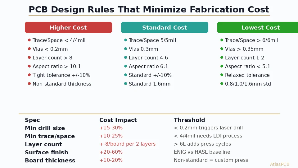
Design Rules for CAF Prevention
Minimum Spacing Rules
The following table provides recommended minimum hole-to-hole spacings based on operating conditions and material class:
| Operating Condition | Standard FR-4 | CAF-Resistant FR-4 | High-Performance Laminate |
|---|---|---|---|
| <30 V, benign environment | 400 µm (16 mil) | 300 µm (12 mil) | 250 µm (10 mil) |
| 30–60 V, controlled environment | 600 µm (24 mil) | 400 µm (16 mil) | 300 µm (12 mil) |
| 60–100 V, humid environment | 800 µm (32 mil) | 500 µm (20 mil) | 400 µm (16 mil) |
| >100 V, harsh environment | 1,000 µm (40 mil)+ | 700 µm (28 mil) | 500 µm (20 mil) |
These are wall-to-wall spacings (edge of one drilled hole to edge of another), not center-to-center.
Note: For standard consumer designs at 3.3 V or 5 V operating voltage, CAF is rarely a concern at normal via spacings. CAF becomes a primary concern for:
- Automotive (high temperature + humidity + vibration)
- Aerospace/military (long life, extreme environments)
- High-voltage applications (power supplies, motor drives, LED drivers)
- Industrial equipment in humid environments
Design Strategies
1. Rotate Drill Patterns Relative to Glass Weave
Glass weave in PCB laminates runs in two perpendicular directions: warp and fill. If a row of vias is aligned perfectly with a fiber bundle, CAF can propagate along the entire bundle. Rotating the via pattern by 10–15° relative to the glass weave direction breaks up the continuous pathway.
In practice, this is difficult to implement because most CAD tools don’t track glass weave orientation. However, staggering vias (offsetting alternate rows) achieves a similar effect.
2. Avoid Dense Via Arrays at Minimum Spacing
BGA fan-out patterns create dense via arrays where many holes at minimum spacing are drilled through the same fiber bundles. If CAF is a concern:
- Use microvias (laser-drilled) instead of through-hole vias — laser drilling doesn’t disrupt fibers the same way
- Increase via-to-via spacing beyond the minimum where possible
- Use via-in-pad to eliminate dog-bone vias that add more holes
3. Separate High-Voltage Nets from Low-Voltage Nets
The voltage gradient drives CAF growth. Maximizing the spacing between high-voltage conductors and low-voltage conductors reduces the driving force. In mixed-voltage designs:
- Route high-voltage traces on dedicated layers
- Use keep-out zones around high-voltage vias
- Consider separate board areas for high-voltage and low-voltage circuits
4. Minimize Mechanical Drilling Where Possible
Laser-drilled microvias create far fewer fiber-disruption initiation sites than mechanical drilling. For CAF-sensitive designs, maximizing the use of HDI technology with laser-drilled vias can significantly reduce CAF risk.
Material Selection for CAF Resistance
Material selection is the most impactful single factor in CAF prevention. The key material properties that enhance CAF resistance are detailed in our [material selection guide]/blog/pcb-material-selection-guide/) and [high-Tg material guide]/blog/high-tg-pcb-material-selection/):
Spread Glass Weave
Standard glass weave (e.g., 7628, 2116, 1080 styles) has rounded fiber bundles with resin-rich channels between them. These channels are the primary CAF propagation pathways.
Spread glass (also called flat glass or open weave) mechanically flattens the fiber bundles, eliminating the resin-rich channels. This:
- Removes the primary CAF pathway
- Improves resin-to-glass ratio uniformity
- Reduces the laminate’s sensitivity to glass weave orientation
Spread glass weave is the single most effective material improvement for CAF resistance. Laminates like Isola 370HR, Panasonic Megtron 6, and Shengyi S1000-2M are available with spread glass options.
High Resin Content
More resin between fiber bundles means fewer dry spots and voids that could serve as CAF pathways. Prepreg with higher resin content (e.g., 60%+ for 1080 style) fills gaps more completely during lamination.
Improved Glass Sizing (Coupling Agent)
The silane coupling agent on glass fibers determines the strength of the glass-resin bond. Advanced sizing formulations provide:
- Better hydrolytic stability (less degradation from moisture)
- Stronger initial bond strength
- Better compatibility with high-Tg resin systems
Low-Moisture-Absorption Resin
Resins that absorb less moisture provide less electrolyte for CAF propagation. Low-Dk/low-Df resins (e.g., polyphenylene ether (PPE), hydrocarbon-based) absorb less moisture than standard DICY-cured epoxy.
Material Comparison for CAF Resistance
| Material | Glass Weave | Resin System | CAF Resistance |
|---|---|---|---|
| Standard FR-4 (Tg 130) | Round bundle | DICY-cured epoxy | Poor |
| Mid-Tg FR-4 (Tg 150) | Round bundle | Modified epoxy | Moderate |
| High-Tg FR-4 (Tg 170+) | Round or spread | Phenolic-cured epoxy | Good |
| Isola 370HR | Spread available | Phenolic-cured epoxy | Very Good |
| Megtron 6 | Spread | Low-loss PPE | Excellent |
| Rogers/PTFE | N/A (woven PTFE) | PTFE | Excellent |
Environmental and Process Controls
Humidity Control
- Manufacturing: Control PCB storage humidity; vacuum-seal boards with desiccant after fabrication
- Assembly: Bake boards per IPC-J-STD-033 before reflow if stored in uncontrolled environments
- End-use: Conformal coating (acrylic, silicone, polyurethane, or parylene) provides an excellent moisture barrier for assembled boards in humid environments
Lamination Process
- Adequate resin flow: Ensure sufficient resin during lamination to fill all gaps at fiber interfaces
- Press temperature uniformity: Uneven heating causes local resin starvation
- Vacuum lamination: Removes trapped air that could create voids along fibers
- Post-cure: Extended post-cure (e.g., 4 hours at 150°C) cross-links the resin further, improving moisture resistance
Drilling Process
- Sharp drill bits: Dull bits create more fiber disruption; replace bits per manufacturer’s recommendations (typically every 2,000–3,000 hits)
- Controlled drill parameters: Entry/retract speed, spindle RPM, and chip load affect fiber disruption
- Backup material: Proper entry and backup materials reduce fiber pullout
CAF Failure Analysis
When CAF is suspected, the following analysis sequence is recommended:
Electrical characterization: Measure insulation resistance between suspect conductors at different voltages and temperatures. CAF shows voltage-dependent, temperature-accelerated behavior.
Cross-sectioning: Microsection the suspect area to look for visible filament growth along glass fibers. May require multiple sections to find the filament.
SEM/EDS analysis: Scanning Electron Microscopy with Energy-Dispersive X-ray Spectroscopy can identify the filament composition (copper) and map it along the fiber-resin interface.
Thermal analysis: TGA/DSC of the laminate can reveal moisture content and degree of cure, which may explain susceptibility.
Industry Trends and Emerging Concerns
Miniaturization Increases CAF Risk
As via-to-via spacing shrinks (driven by finer BGA pitches and higher layer counts), the safety margin against CAF decreases. What was a 1.0 mm via pitch ten years ago is now 0.5 mm or even 0.4 mm. At these spacings, CAF can bridge between conductors in months rather than years.
Lead-Free Assembly Increases Thermal Stress
Lead-free reflow temperatures (peak ~260°C vs. ~225°C for leaded) create more thermal stress on the glass-resin interface, increasing the likelihood of interface separation that enables CAF.
Electric Vehicle and Renewable Energy Applications
High-voltage PCBs for EV inverters (400–800 V bus) and solar inverters face extreme CAF risk due to high voltage gradients combined with harsh thermal environments. These applications are driving demand for CAF-resistant materials.
Conformal Coating as a Defense
For assembled boards, conformal coating is emerging as a cost-effective defense layer. Parylene coating, in particular, provides an excellent moisture barrier that dramatically reduces the electrolyte available for CAF formation.
Summary
CAF is a serious but preventable reliability threat. The key principles:
- Understand the mechanism: CAF requires pathway + moisture + voltage — eliminate any one to prevent it
- Select appropriate materials: Spread glass weave is the single most effective countermeasure
- Design with adequate spacing: Follow voltage-dependent spacing rules; increase spacing for harsh environments
- Control humidity: Proper storage, bake-out, and conformal coating
- Minimize mechanical drilling disruption: Use laser-drilled microvias where possible
- Test and validate: IPC-TM-650 2.6.25 at conditions representative of your end-use environment
For high-reliability applications — automotive, aerospace, medical, industrial — CAF resistance should be part of the design specification from day one, not an afterthought when field failures appear.
Ready to start your project? Upload your Gerbers for a free engineering review, or talk to an engineer about your design requirements.
Further Reading
- [PCB Rigid-Flex Bend Zone Reliability: Design Rules, Material Selection & Lifecycle Testing]/blog/pcb-rigid-flex-bend-zone-reliability/)
- [PCB Design for GaN and SiC Power Devices: Thermal Management, Layout Rules, and Material Selection]/blog/pcb-design-gan-sic-power-devices-thermal-layout/)
- [PCB Panelization and Array Design: V-Score vs Tab Routing, DFM Rules, and Cost Optimization]/blog/pcb-panelization-v-score-tab-routing-dfm-cost-optimization/)
- [mmWave PCB Material Selection: Rogers vs Megtron vs LCP for 5G and 6G Applications]/blog/mmwave-pcb-material-selection-rogers-megtron-lcp-5g-6g/)
- [Rogers PCB Fabrication: Material Sourcing, Lead Times & Quality Control]/blog/rogers-pcb-fabrication/)
- Our Manufacturing Capabilities
About AtlasPCB — We specialize in complex PCB manufacturing for HDI, RF, and high-reliability applications. Explore our impedance-controlled PCB manufacturing . Every order includes free engineering review. Get your quote.
Reviewed by AtlasPCB Engineering Team — IPC-certified manufacturing specialists with 15+ years of production experience in HDI, RF, and high-reliability PCB fabrication. Content based on factory floor data and real customer design reviews.
- caf
- reliability
- electrochemical-migration
- pcb-materials
- design-rules