· AtlasPCB Engineering · Engineering · 9 min read
PCB Thermal Design for AI Inference Accelerators: Managing 50-150W in Edge Deployments
AI inference hardware pushes PCB thermal management beyond standard techniques. This guide covers the specific stackup, via, and material strategies needed for AI accelerator boards dissipating 50-150W without server-class cooling infrastructure.
The Thermal Challenge in Edge AI
Server-class AI hardware solves thermal management through brute force: 200-400 CFM airflow, vapor chambers, and liquid cooling loops. When the same inference workload moves to edge deployments — retail kiosks, autonomous vehicles, factory floors, telecommunications cabinets — the cooling budget drops dramatically while the silicon’s thermal dissipation remains unchanged.
An NVIDIA Orin dissipates 15-75W depending on workload. Intel’s Meteor Lake with NPU reaches 28-45W. Custom ASICs for specific inference tasks (object detection, NLP) commonly land in the 30-80W range. Edge AI modules stacking multiple accelerators can push total board dissipation beyond 150W in a fanless or low-airflow enclosure.
At these power levels, the PCB thermal design is not optional — it is a critical system component. A poorly designed board (insufficient thermal vias, thin copper planes, no thermal simulation) can add 15-30C to junction temperature, pushing the silicon out of spec and triggering thermal throttling that defeats the purpose of dedicated acceleration hardware.
Based on AI inference boards we have fabricated over the past 18 months, the designs that succeed in edge thermal environments share three characteristics: dense thermal via arrays under all power dissipation sites, heavy copper inner planes (2-3oz) for lateral heat spreading, and board-level thermal simulation informing the layout before routing begins.
AI HARDWARE PCB SPECIALIST
High-Power AI Board Fabrication — Thermal Via Arrays, Heavy Copper, HDI
We fabricate AI inference boards with up to 5oz copper, plated-shut thermal via arrays, and HDI via-in-pad construction. 8 to 30 layers with controlled impedance for high-speed memory interfaces.
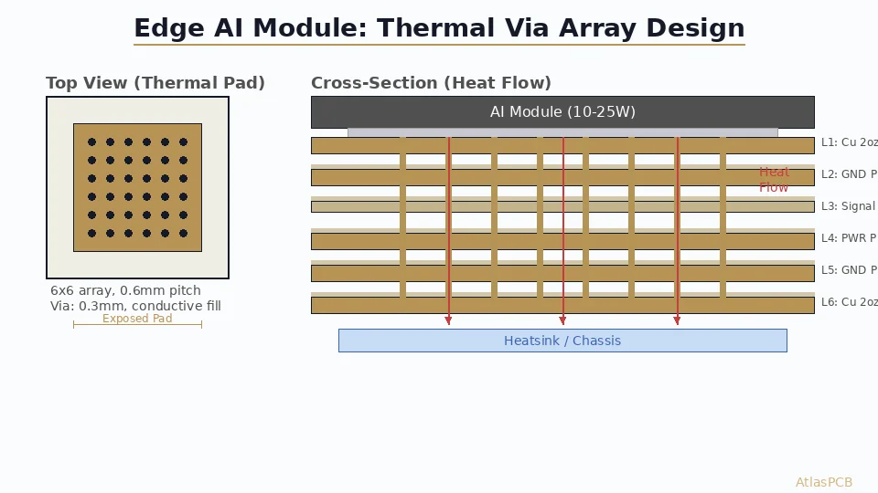
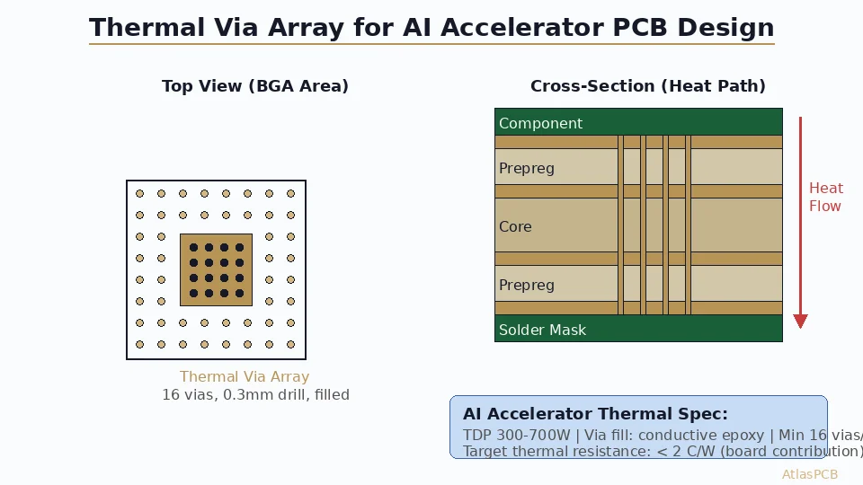
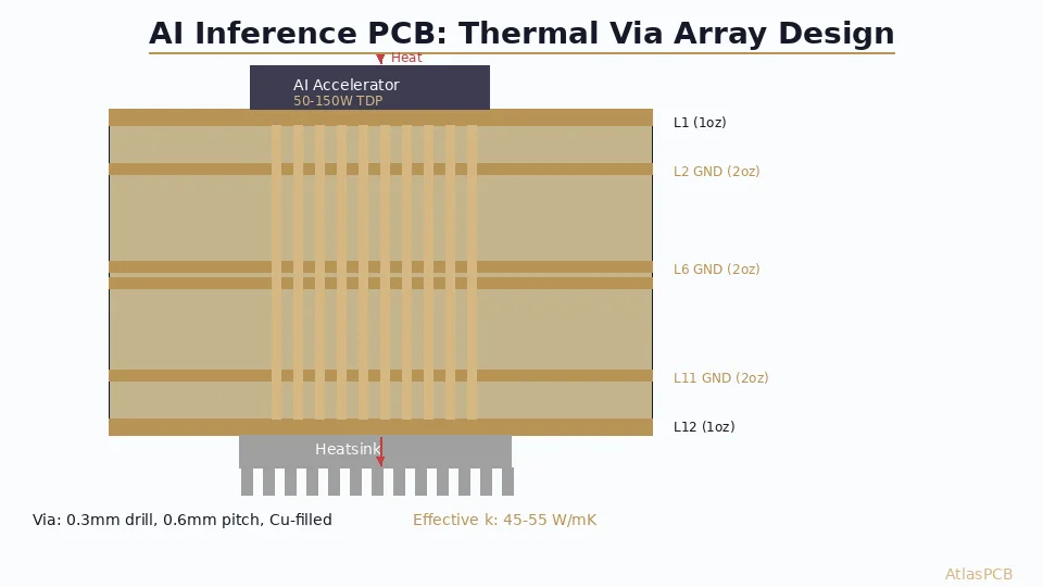
Thermal Via Array Design: The Numbers That Matter
Thermal vias are the primary mechanism for moving heat from the component side of the PCB to the opposite side (where heatsinks typically mount). The effectiveness depends on via diameter, pitch, plating thickness, and fill material.
Via Parameters and Thermal Resistance
| Via Configuration | Via Density (per cm2) | Effective k (W/mK) | For 50W over 15x15mm | Notes |
|---|---|---|---|---|
| 0.3mm drill, 0.6mm pitch, plated-shut | 278 | 45-55 | Delta-T: 12-16C | Best cost/performance |
| 0.2mm drill, 0.5mm pitch, plated-shut | 400 | 55-65 | Delta-T: 9-13C | HDI-level density |
| 0.3mm drill, 0.6mm pitch, hollow | 278 | 15-25 | Delta-T: 25-40C | Air gap limits performance |
| 0.1mm laser via, 0.25mm pitch, Cu-filled | 1600 | 70-90 | Delta-T: 6-9C | HDI required, expensive |
The critical distinction: plated-shut (copper-filled) vias versus hollow vias. A hollow via contains trapped air with thermal conductivity of 0.025 W/mK — effectively an insulator. Filling the via with copper increases effective Z-axis conductivity by 3-4x. For AI boards dissipating above 30W per component, copper-filled vias are mandatory, not optional.
In our production process, via filling uses a conductive paste or electroplated copper fill followed by surface planarization (cap plating). The planarized surface is critical for two reasons: it enables surface-mount components directly over filled vias (via-in-pad), and it eliminates the dimple that would trap air and degrade thermal contact with the component.
Via Array Sizing
The thermal via array should extend slightly beyond the component’s thermal pad area. For an AI accelerator with a 15x15mm exposed pad:
- Minimum via array: 15x15mm (matches pad exactly)
- Recommended: 17x17mm (1mm extension per side for thermal spreading)
- Optimal: extend to nearest ground plane boundary or power island edge
Vias outside the thermal pad area still contribute to heat spreading through lateral copper connections on inner planes. The diminishing-returns point is approximately 1.5x the thermal pad area — beyond this, additional vias add cost without meaningful temperature reduction.
THERMAL VIA PROCESSING
Plated-Shut Thermal Vias with Via-in-Pad Planarization
Copper-filled vias with surface planarization — enabling dense thermal arrays directly under BGA pads. Up to 16:1 aspect ratio, minimum 0.15mm drill.
Upload Design ›Stackup Architecture for Thermal Performance
The ideal AI inference board stackup balances three requirements: signal routing density (HDI for BGA fanout), power delivery (low-impedance PDN), and thermal management (heavy copper planes as heat spreaders).
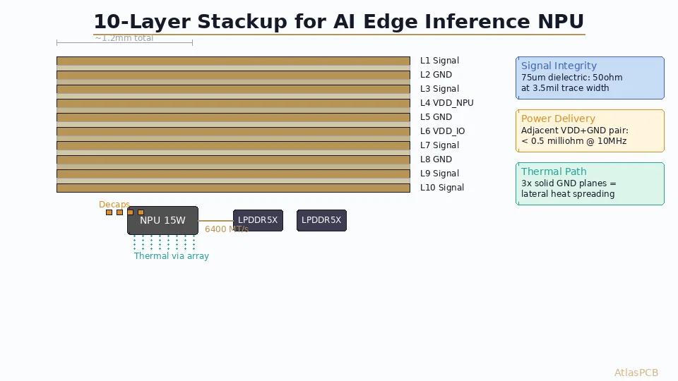
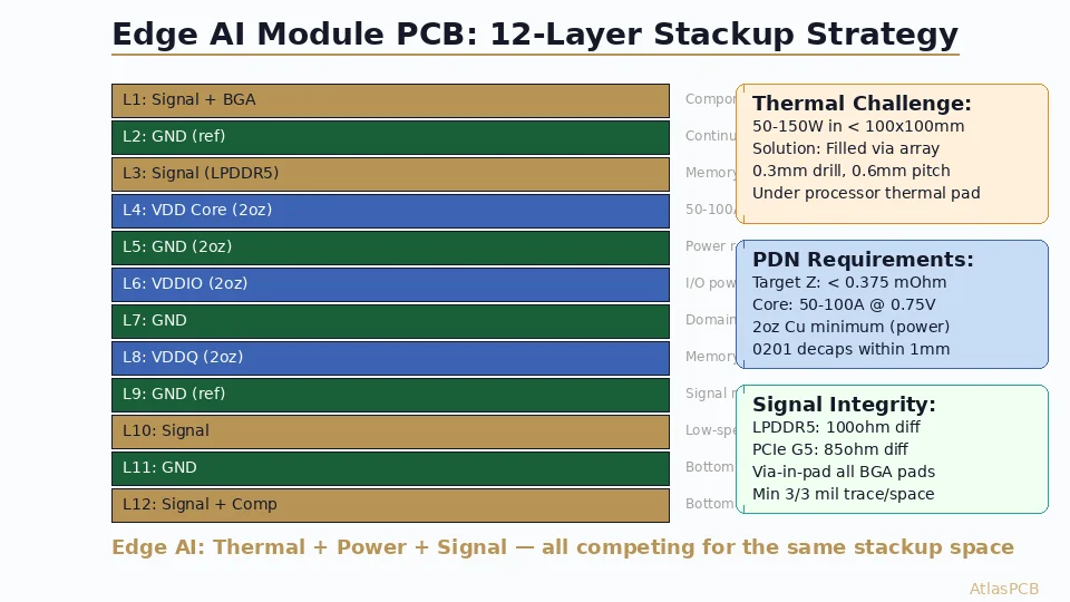
Recommended 12-Layer AI Inference Stackup
L1:  Signal (BGA fanout) — 1oz Cu, microstrip
     Core: High-Tg FR-4, 3.5mil
L2:  Ground Plane — 2oz Cu (thermal spreader)
     Prepreg: 4mil
L3:  Signal (high-speed routing) — 1oz Cu
     Core: 4mil
L4:  Power Plane — 2oz Cu (thermal spreader + PDN)
     Prepreg: 4mil
L5:  Signal (DDR routing) — 1oz Cu
     Core: 4mil
L6:  Ground Plane — 2oz Cu (thermal spreader)
     Prepreg: 4mil (center)
L7:  Ground Plane — 2oz Cu (thermal spreader)
     Core: 4mil
L8:  Signal (slow digital, I2C, SPI) — 1oz Cu
     Prepreg: 4mil
L9:  Power Plane — 2oz Cu (PDN)
     Core: 4mil
L10: Signal (routing) — 1oz Cu
     Prepreg: 4mil
L11: Ground Plane — 2oz Cu (thermal spreader)
     Core: 3.5mil
L12: Signal (bottom components) — 1oz Cu
Total board thickness: approximately 2.0mm with 2oz inner copper. The four 2oz ground/power planes provide continuous lateral heat spreading from the via array to the board edges, where heat transfers to the enclosure or heatsink mounting points.
Why 2oz Inner Copper Matters
Copper’s thermal conductivity (385 W/mK) is nearly 1000x that of FR-4 (0.3-0.4 W/mK). At 2oz (70μm) thickness per plane, each copper layer acts as a heat spreader carrying thermal energy laterally from the hot zone to cooler board areas. The temperature gradient across a 2oz plane dissipating 50W laterally is approximately 3-5C over 30mm of spreading distance — compared to 15-25C in 1oz copper for the same configuration.
Going from 1oz to 2oz inner copper typically adds 20-30% to board cost but can reduce junction temperature by 8-15C. For AI inference boards operating near thermal limits, this cost is almost always justified by the reliability improvement (every 10C reduction roughly doubles semiconductor lifetime per Arrhenius relationship).
HDI Integration for AI Accelerator Packages
Modern AI inference chips use BGA packages with 0.5-0.8mm ball pitch. At 0.5mm pitch, standard mechanical drill (minimum 0.15mm via in 0.3mm pad) cannot route escape signals between BGA pads — HDI with laser-drilled microvias (0.075-0.1mm) becomes mandatory.
The HDI construction provides a thermal bonus: copper-filled microvias in a via-in-pad configuration create a direct thermal path from the BGA thermal pad through the first core to the L2 ground plane. Combined with mechanical thermal vias from L2 to L12, this creates an uninterrupted copper thermal conduit from component to heatsink.
A typical AI board HDI configuration:
- 1+N+1 or 2+N+2 buildup for BGA fanout
- Via-in-pad with copper fill on all thermal pad vias
- Stacked microvias connecting L1-L2-L3 for maximum thermal density
- Back-drilled through-vias from L3-L12 for thermal and signal purposes
The additional cost of HDI construction (25-40% over standard through-hole) is often already required for signal routing at fine BGA pitch. Designing the thermal via strategy into the HDI structure from the beginning — rather than treating thermal management as an afterthought — leverages the HDI investment for both electrical and thermal benefit.
HDI PCB MANUFACTURER
HDI Up to 5+N+5 — Via-in-Pad, Stacked Microvias, Copper Fill
We fabricate HDI boards from 1+N+1 through 5+N+5 buildup with copper-filled vias, BGA escape routing at 0.5mm pitch, and controlled impedance for DDR5 and PCIe Gen5 interfaces.
Get HDI Quote ›Power Delivery Network: Supporting AI Accelerator Current Draw
AI inference chips draw substantial current — a 75W chip at 0.85V core voltage requires 88A. This current must be delivered through the PCB’s power distribution network (PDN) with sufficiently low impedance to avoid voltage droop during processing bursts.
The PDN requirements for AI inference boards:
- Target impedance: typically <1 milliohm from 100 kHz to 100 MHz
- Decoupling strategy: bulk capacitors (100-330μF) at 2-5mm from BGA, MLCC (100nF-10μF) at <1mm from power pins
- Copper pour connectivity: 2oz power planes with multiple via connections to BGA power pins
- Voltage regulator placement: within 15mm of BGA to minimize high-current path length
The thermal and PDN requirements are synergistic: heavy copper planes serve both functions simultaneously. A 2oz power plane that delivers current also spreads heat. The board designer should co-optimize these functions rather than treating them independently.
Manufacturing Considerations for AI Thermal Boards
Process Challenges
Dense thermal via arrays create manufacturing challenges that not all fabricators handle well:
- Drill accuracy in arrays: 600+ vias in a 17x17mm area requires consistent drill positioning without bit wander. Worn drill bits in the interior of large arrays can drift, creating incomplete plating.
- Plating uniformity: Copper electroplating must fill all vias completely. Under-filled vias in the array center (where plating solution exchange is poorest) create thermal weak spots.
- Registration with HDI layers: Thermal via arrays must align with BGA pad patterns from HDI layers above. Misregistration between mechanical drill and laser drill layers must be <50μm.
- Heavy copper etching: 2-3oz inner copper requires different etch chemistry and timing. Fine traces on heavy copper layers need careful compensation — minimum trace width on 2oz copper is typically 5/5mil versus 3/3mil on 1oz.
What to Specify in Your Fabrication Notes
For AI inference boards with critical thermal requirements, include in your fab drawing:
- Via fill requirement: “All thermal vias must be copper-filled and planarized to ±10μm”
- Copper weight callout per layer: specify 2oz or 3oz on thermal spreading layers
- Via array inspection: “100% visual inspection of thermal via array plating”
- Material: “High-Tg FR-4, Tg ≥ 170C, Td ≥ 340C”
- Cross-section requirement: “Provide micro-section of thermal via area in first article”
ATLASPCB
Building AI Inference Hardware? Get Your PCB Right First.
Upload your AI accelerator board design for thermal-aware DFM review. We identify thermal via density issues, copper weight optimization, and HDI routing strategies — before fabrication.
Get AI Board Quote ›Reviewed by AtlasPCB Engineering Team — 15+ years in advanced PCB fabrication for RF, HDI, and rigid-flex applications.
Related Reading:
About AtlasPCB — We specialize in complex PCB manufacturing for HDI, RF, and high-reliability applications. Explore our HDI PCB manufacturing capabilities, multilayer PCB fabrication up to 30 layers, or get an aluminum and metal-core PCB services . Every order includes free engineering review. Get your quote.
Reviewed by AtlasPCB Engineering Team — IPC-certified manufacturing specialists with 15+ years of production experience in HDI, RF, and high-reliability PCB fabrication. Content based on factory floor data and real customer design reviews.
- AI hardware PCB
- thermal management PCB
- HDI PCB manufacturer
- PCB stackup design guide
- thermal via
- edge AI