· AtlasPCB Engineering · Engineering · 7 min read
PCB Edge Plating and Castellated Holes: Complete Guide to Module-Ready Board Design
Master PCB edge plating and castellated hole design for modular electronics. Learn manufacturing processes, IPC specifications, design rules, and solderability requirements for reliable board-to-board connections.
What Is PCB Edge Plating?
PCB edge plating is a manufacturing process that deposits copper onto the machined edges of a circuit board, creating electrically conductive and solderable surfaces along the board perimeter. This technique serves two primary purposes: providing ground shielding for EMI-sensitive designs and enabling board-to-board electrical connections without connectors.
Unlike standard through-hole plating that coats only internal barrel walls, edge plating wraps copper around the board’s cut edges. The resulting metallized edge can be soldered directly to an adjacent board, chassis, or RF enclosure.
Edge Plating vs. Castellated Holes
While related, these are distinct techniques:
| Feature | Edge Plating | Castellated Holes |
|---|---|---|
| Geometry | Flat metallized edge | Half-barrel (semicircular) pads at edge |
| Primary use | EMI shielding, grounding | Module-to-carrier board connections |
| Signal routing | Rarely (ground only) | Yes — individual signal/power pads |
| Minimum pitch | N/A (continuous) | 1.0 mm recommended |
| IPC reference | IPC-6012 4.3.7 | IPC-6012 3.6.2.12 |
Castellated Hole Design Rules
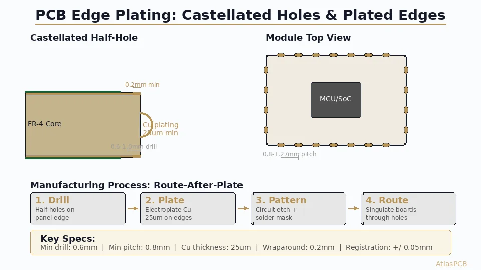
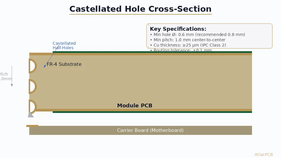
Castellated holes (also called castellations, half-holes, or plated half-vias) are formed by drilling plated through-holes at the board edge and then routing through their center. The result is a half-barrel of plated copper exposed at the board outline.
Critical Dimensions
Hole diameter: Minimum 0.6 mm finished diameter. For best plating uniformity, use ≥ 0.8 mm. The half-barrel after routing will be exactly half of the drilled diameter.
Pitch: Minimum 1.0 mm center-to-center. Tighter pitches (down to 0.8 mm) are achievable but increase cost and reduce yield.
Copper thickness: Minimum 25 µm in the barrel per IPC-6012 Class 2. For Class 3 (high-reliability), specify ≥ 30 µm with no voids exceeding 5% of barrel circumference.
Board thickness: 0.8–2.4 mm. Thinner boards (< 0.8 mm) risk cracking during half-hole routing. Thicker boards (> 2.4 mm) make soldering the module to carrier board difficult due to excessive fillet height requirements.
Edge-to-hole tolerance: The routing bit must cut exactly through the hole center. Specify ±0.1 mm tolerance on the routing path relative to drill position.
Design for Manufacturing (DFM) Guidelines
Pad annular ring: Maintain minimum 0.15 mm annular ring on the internal pad connected to the castellated hole. This ensures the copper barrel remains bonded to internal traces during routing.
Solder mask clearance: Keep solder mask at least 0.1 mm away from the castellated hole edge. Mask over the half-barrel prevents soldering.
Copper pullback: On non-castellated edges, pull copper planes back 0.3–0.5 mm from the board edge to prevent copper burrs and delamination.
Breakout tabs: When panelized, place V-score or tab-route breakout points away from castellated edges. Routing vibration near castellations can fracture the thin plated barrel.
Test points: Include at least one castellated hole connected to a known net for in-circuit testing of the plating continuity.
Manufacturing Process
Edge Plating Process Flow
Panel drill → PTH plating → Pattern plate → Edge route (expose copper at edge)
→ Secondary plating (optional) → Surface finish → Final profile route
The critical step is the initial edge route that exposes the copper at the board perimeter while maintaining panel integrity. Manufacturers typically use a two-stage routing process:
- First route: Cuts a channel exposing the edge copper while leaving tabs to hold the panel together
- Plating/finish: Applied to the exposed edge along with the rest of the board
- Final route: Separates individual boards from the panel
Castellated Hole Process Flow
Drill PTH at board edge positions → Electroless copper → Electrolytic copper plate
→ Pattern/etch circuit layers → Apply solder mask (clear of half-holes)
→ Surface finish → Route through hole centers → Depanel
The routing-through-hole step is the most critical. The router bit (typically 1.0–2.0 mm diameter) must track precisely through each hole center. Misalignment by more than ±0.1 mm creates an asymmetric half-barrel that affects solderability.

Need Castellated Hole PCBs for Your Module Design?
AtlasPCB manufactures castellated-hole and edge-plated boards with ≥25 µm copper barrel thickness, ±0.1 mm routing precision, and 100% optical inspection. Get DFM feedback within 24 hours.
Request a Quote →Surface Finish Selection for Castellated Holes
The surface finish on castellated half-barrels directly impacts solderability during module attachment. Not all finishes perform equally:
| Finish | Shelf Life | Solderability | Recommended? |
|---|---|---|---|
| ENIG | 12+ months | Excellent | ✅ Best choice |
| Immersion Tin | 6 months | Good | ✅ Good for cost-sensitive |
| HASL (lead-free) | 12 months | Fair (uneven) | ⚠️ Barrel bridging risk |
| OSP | 6 months | Poor on half-barrel | ❌ Not recommended |
| Hard Gold | 12+ months | Excellent | ✅ Premium option |
ENIG (Electroless Nickel Immersion Gold) is the preferred finish because:
- Uniform thickness on complex geometries including half-barrels
- Excellent wetting with both leaded and lead-free solder
- Long shelf life for modules stored before assembly
- No coplanarity issues common with HASL on half-holes
Soldering Castellated Modules
Reflow Profile Considerations
When soldering a castellated module onto a carrier board, the thermal mass of two boards must be considered:
- Preheat: Extend preheat zone by 30–60 seconds to equalize temperature across both boards
- Peak temperature: Standard SAC305 profiles (245°C peak) work well
- Solder paste: Use Type 4 or finer paste on the carrier board landing pads
- Stencil thickness: 0.12–0.15 mm for castellated landing pads
Landing Pad Design on Carrier Board
The carrier board (motherboard) must have landing pads that extend beyond the module outline:
- Pad extension: 0.3–0.5 mm beyond module edge (outward) for fillet inspection
- Pad width: Match the castellated hole diameter ± 0.1 mm
- Pad length (under module): 0.5–1.0 mm for mechanical strength
- Thermal relief: Use solid connections (no thermal relief) on landing pads for better heat transfer during reflow
IPC Specifications and Standards
IPC-6012 Requirements
Section 3.6.2.12 covers plated edges and castellated holes:
- Minimum copper: 20 µm (Class 1), 25 µm (Class 2), 30 µm (Class 3)
- Void allowance: ≤ 10% of barrel length (Class 2), ≤ 5% (Class 3)
- Edge roughness: Ra ≤ 25 µm after routing
- Copper adhesion: No peeling or lifting when tested per IPC-TM-650 2.4.1
IPC-7093 (Bottom Termination Components)
While primarily for BTC/QFN packages, IPC-7093 provides relevant solder joint criteria for castellated modules:
- Minimum fillet height: 25% of module board thickness
- Minimum fillet width: Visible fillet at pad edge
- Heel fillet: Must be visible (non-zero) for Class 3
Common Defects and Prevention
1. Copper Void in Half-Barrel
Cause: Poor plating solution penetration into partial holes during electroplating.
Prevention:
- Use pulse plating rather than DC plating for half-holes
- Specify solution agitation directed at board edges
- Design castellated holes ≥ 0.8 mm for better throwing power
2. Barrel Crack After Routing
Cause: Mechanical stress from routing bit vibration fracturing thin copper.
Prevention:
- Route at reduced feed rate (50% of normal) near castellations
- Use climb milling rather than conventional milling
- Specify minimum 25 µm copper (not 20 µm) for routing robustness
3. Solder Bridging Between Castellations
Cause: Pitch too tight or excessive solder paste on carrier board.
Prevention:
- Maintain ≥ 1.0 mm pitch for standard assemblies
- Use step-down stencil with 0.10 mm thickness in castellated pad region
- Apply solder mask dam between landing pads (minimum 0.15 mm dam width)
4. Poor Wetting on Half-Barrel
Cause: Oxidation of copper edge or contamination from routing debris.
Prevention:
- Apply surface finish after final routing (not before)
- Clean routed edges with DI water rinse before finish application
- Avoid OSP finish on castellated holes (insufficient protection of exposed copper)
Application Examples
WiFi/Bluetooth Modules
Most WiFi/BT modules (ESP32, nRF52, Realtek RTL8720) use castellated holes:
- Typical pitch: 1.27 mm
- Hole diameter: 0.8–1.0 mm
- Board thickness: 0.8–1.0 mm
- Finish: ENIG
LoRa/LPWAN Modules
Semtech SX1276-based modules commonly use castellations:
- Pitch: 1.0–1.27 mm
- Additional ground castellation on RF shielding edge
- Thicker boards (1.2 mm) for antenna impedance control
Power Supply Modules
DC-DC converter modules require heavy current through castellations:
- Larger holes: 1.0–1.5 mm for power pins
- Multiple paralleled castellations for high-current paths (>3A per pin)
- Thermal pad (large copper area) at module center for heat dissipation
Design Checklist
Before releasing your castellated hole design to manufacturing, verify:
- All castellated holes ≥ 0.6 mm (preferably ≥ 0.8 mm)
- Center-to-center pitch ≥ 1.0 mm
- Solder mask clearance ≥ 0.1 mm from half-barrel edge
- Internal annular ring ≥ 0.15 mm maintained
- Routing tolerance specified as ±0.1 mm
- Copper thickness callout ≥ 25 µm (barrel)
- Surface finish specified (ENIG recommended)
- Carrier board landing pads extend 0.3–0.5 mm beyond module edge
- No copper pour within 0.3 mm of non-castellated board edges
- Panelization breakout tabs away from castellated edges
- Test coupon included for plating thickness verification
Further Reading
- PCB Surface Finish Comparison: ENIG, HASL, OSP, and More
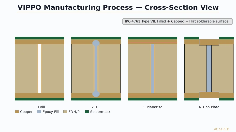
- Via-in-Pad Plated Over (VIPPO) Design Guide
- PCB Panelization Guide: V-Score, Tab Routing, and DFM
- DFM for Fine-Pitch BGA: Design Rules and Best Practices
Need expert support for your castellated hole or edge-plated PCB design? Contact AtlasPCB Engineering for a free DFM review and competitive quote on module-ready boards with guaranteed plating quality.
About AtlasPCB — We specialize in complex PCB manufacturing for HDI, RF, and high-reliability applications. Explore our RF and high-frequency PCB services, PCB assembly services, or get an free engineering DFM review . Every order includes free engineering review. Get your quote.
Reviewed by AtlasPCB Engineering Team — IPC-certified manufacturing specialists with 15+ years of production experience in HDI, RF, and high-reliability PCB fabrication. Content based on factory floor data and real customer design reviews.
- PCB edge plating
- castellated holes
- module design
- board-to-board connection
- soldering
- DFM
- PCB manufacturing
- surface mount modules
- half-hole plating
- IPC standards