· AtlasPCB Engineering · Engineering · 11 min read
PCB Thermal Design for AI Edge Inference Accelerators: Managing 15-75W in Compact Form Factors
Engineering guide to PCB thermal management for edge AI inference hardware. Covers power delivery network design, thermal via arrays, material selection, and stackup optimization for AI SoCs dissipating 15-75W in space-constrained edge deployments without server-class cooling.
The Edge AI Thermal Challenge: No Server Fans Allowed
| Parameter | Data Center AI PCB | Edge AI Inference PCB |
|---|---|---|
| Power budget | 300-1000W (GPU board) | 15-75W (SoC + memory) |
| Cooling method | Active forced air (30-60 CFM) | Conduction + natural convection |
| Ambient temperature | 25-35C (controlled) | 0-55C (uncontrolled) |
| PCB size | 300x300mm+ (no constraint) | 80x120mm typical (enclosure-limited) |
| Airflow over board | 2-5 m/s minimum | 0-1 m/s (sealed or fanless) |
| Junction temp budget | 95-105C (Tj,max - T,ambient) | 50-80C (much tighter) |
| Layers | 16-24 | 8-12 |
The fundamental difference: Data center AI boards dissipate heat primarily through forced airflow over heatsink fins. Edge AI boards must conduct heat through the PCB itself to a chassis or enclosure surface. This makes PCB thermal design the primary thermal management mechanism, not a secondary consideration.
Power Density Reality at the Edge
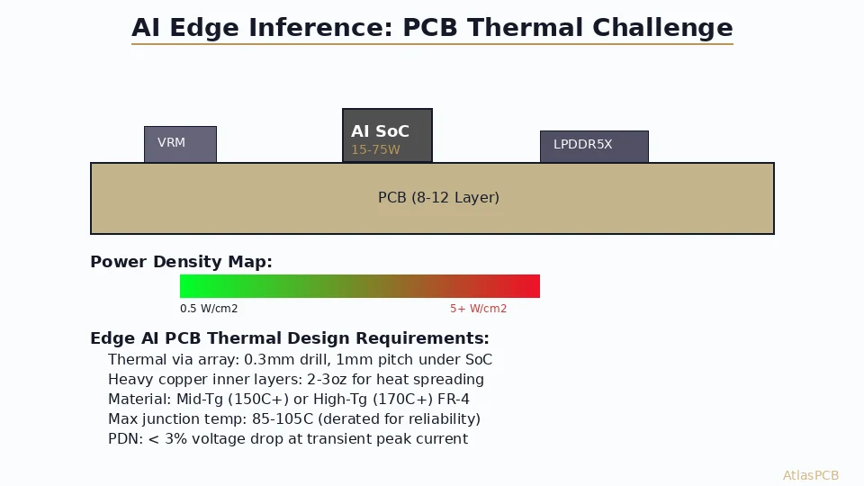
Edge AI inference is experiencing a rapid convergence of increasing compute power and decreasing physical size that creates unprecedented PCB thermal challenges. Today’s edge inference SoCs — devices like the Hailo-15, NVIDIA Jetson Orin NX, Qualcomm Cloud AI 100 Edge, and Intel Meteor Lake with NPU — pack 15-75W of thermal dissipation into BGA packages with thermal pad areas of 15x15mm to 35x35mm. That translates to power densities of 1.5-5.5 W/cm2 at the package level, concentrated into the PCB thermal pad zone.
For comparison, a standard FR-4 board without thermal management reaches approximately 60C temperature rise per W/cm2 in still air. At 3 W/cm2 (a modest 45W SoC on a 25x25mm pad), that is a 180C temperature rise — obviously unacceptable. The PCB design must reduce this thermal resistance by a factor of 5-10x through thermal vias, heavy copper planes, and conduction paths to external surfaces.
In our production experience across edge AI platforms, the designs that succeed thermally share three common characteristics: aggressive thermal via arrays under the SoC (achieving less than 3 C/W board-level thermal resistance), internal copper planes at 2-3oz weight extending well beyond the chip footprint, and a clear conduction path from the bottom of the board to a metal chassis or heatsink surface through thermal interface material. Designs that attempt to rely on surface-side convection alone invariably exceed junction temperature limits in sealed enclosures above 40C ambient.
The PDN (power delivery network) design is equally critical and often the actual thermal constraint. A 75W SoC running at 0.8V core voltage draws approximately 90A at the die. The I2R losses in the power delivery path — VRM output capacitors, PCB planes, package redistribution layers — can easily add 5-10W of additional heat distributed across the board. This parasitic heating occurs precisely in the copper planes and vias that you are also counting on for thermal spreading, creating a coupled thermal-electrical design problem that must be solved simultaneously.
AI HARDWARE PCB EXPERTS
Building Edge AI Hardware? Start with the Right PCB.
8-12 layer boards with 2-3oz copper, thermal via arrays, and controlled impedance for high-speed memory interfaces. Stackup engineering included with your first quote.
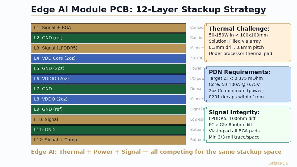
Get AI Board Quote ›Stackup Architecture for Edge AI: The 10-Layer Sweet Spot
Through dozens of edge AI board designs we have manufactured, the 10-layer stackup has emerged as the optimal balance between cost, thermal performance, and signal integrity for the 25-60W power class. Here is the reference stackup our applications engineers typically recommend:
| Layer | Function | Copper Weight | Notes |
|---|---|---|---|
| L1 | Signal + Component | 1oz (finished 1.5oz after cap plating) | SoC fanout, RF/analog if present |
| L2 | Ground (reference) | 2oz | Primary ground reference, thermal spreading |
| L3 | Signal (high-speed) | 1oz | DDR5/LPDDR5X memory interfaces |
| L4 | Power (VDD_CORE) | 2oz | AI SoC core supply, low impedance |
| L5 | Ground (shield) | 2oz | Isolation between power domains |
| L6 | Power (VDD_IO, peripherals) | 2oz | I/O rails, memory power |
| L7 | Signal (low-speed) | 0.5oz | GPIO, I2C, SPI, configuration |
| L8 | Ground (thermal) | 3oz | Primary thermal spreading plane |
| L9 | Signal + Power (aux) | 1oz | Secondary routing, auxiliary power |
| L10 | Ground + Thermal pad | 2oz | Board-to-chassis thermal interface |
The key design choices in this stackup are the heavy copper on layers 2, 4, 5, 6, 8, and 10. These 2-3oz planes serve dual purposes: they provide the low-impedance power delivery that a high-current AI SoC demands, and they simultaneously act as heat spreading layers that conduct thermal energy laterally from the concentrated heat source to the board edges and mounting interfaces.
Layer 8 at 3oz copper is specifically optimized for thermal spreading. At 105um thickness, a 3oz copper plane has lateral thermal conductivity equivalent to a 0.4mm aluminum plate — and because it is embedded within the PCB lamination, it requires no additional assembly steps or thermal interface layers. The thermal via array under the SoC connects through all internal planes, creating a multi-path thermal bus from the component side to the chassis-mounting side.
Material selection for this stackup should be high-Tg FR-4 (Tg 170C minimum, Td 340C+) for all layers. The sustained operating temperatures near the SoC zone — which can reach 90-100C on the copper planes adjacent to the thermal pad — exceed the safe continuous operating range of standard Tg-150 material. For designs pushing beyond 60W or operating in elevated ambient temperatures, specify EM-370D, IS410, or equivalent Tg-180 material for the full stackup.
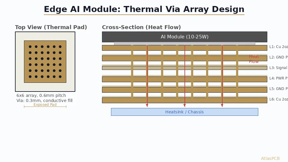
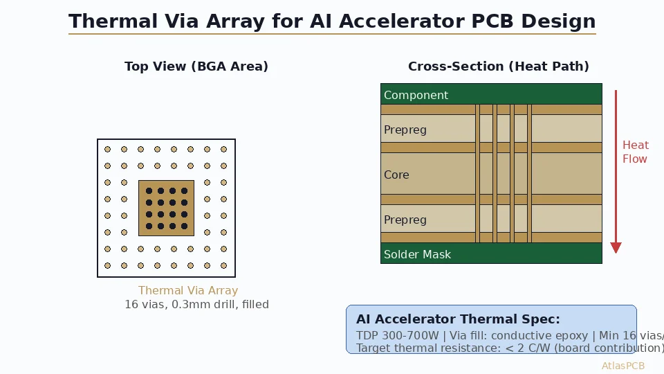
Thermal Via Array Design: The Numbers That Matter
The thermal via array under the AI SoC is the single most impactful thermal design feature on the PCB. Getting this right reduces board-level thermal resistance by 3-5x compared to a board without thermal vias. Getting it wrong — insufficient density, unfilled vias, or poor connection to spreading planes — leaves 10-20C of junction temperature on the table.
Our thermal simulation and measurement correlation across edge AI boards shows the following design rules produce consistently good results:
For a thermal pad area of A cm2, the thermal via array should fill 80-90% of that area (leaving 10-20% for signal breakout routing and mechanical keep-outs). Via drill diameter of 0.3mm with copper fill (IPC-4761 Type VII) provides optimal thermal conductivity per unit area. Smaller drills (0.2mm) have higher fill reliability but lower per-via thermal capacity; larger drills (0.4mm) carry more heat individually but reduce available routing density. At 1.0mm pitch, a 20x20mm thermal pad area contains approximately 360 thermal vias — each contributing roughly 0.015 W/K to the total thermal conductance through the board.
The aggregate thermal resistance of a well-designed via array on a 1.6mm, 10-layer board with 2-3oz internal planes is 1.5-3.0 C/W for a typical 25x25mm SoC footprint. At 50W dissipation, this translates to a 75-150C temperature difference from top copper to bottom copper — which sounds alarming until you recognize that the thermal spreading into adjacent planes reduces this significantly. The actual measured temperature difference between SoC thermal pad and board bottom at the same location is typically 30-50C in our production boards, because 60-70% of the heat spreads laterally into the 2-3oz planes before reaching the bottom.
One design pitfall we catch frequently in DFM review: engineers place thermal vias but forget to connect them to all internal ground/power planes. A 0.3mm via that passes through eight layers but is only connected (non-isolated) to layers 1, 5, and 10 has roughly 40% of the thermal capacity of the same via connected to all eight copper layers. Ensure your Gerber files show clearance-free connections (thermal reliefs removed) between thermal vias and every internal plane they intersect.
HEAVY COPPER + THERMAL VIAS
10-12 Layer Boards with 2-3oz Copper and Filled Via Arrays
Purpose-built for edge AI thermal challenges. We verify your thermal via connectivity to all planes during DFM review — catching the most common heat-related design errors before production.
Upload Your AI Board Design ›PDN Design: Delivering 50-90A to an 0.8V AI Core
The power delivery network for edge AI SoCs is arguably more challenging than data center GPU boards on a per-watt basis, because edge designs have tighter space constraints that force VRM placement further from the die, fewer available power plane layers, and lower copper weights dictated by board thickness limits. A 75W SoC at 0.8V core voltage draws 93A peak — and the entire PDN path from VRM output to die must maintain less than 25mV of DC drop plus less than 40mV of AC ripple to meet typical SoC power integrity specifications.
The critical PDN design parameters for edge AI boards:
VRM placement: The multiphase buck converter must be placed within 10-15mm of the SoC power pins. Every additional millimeter of PCB trace/plane between VRM output and SoC increases both DC resistance and loop inductance. In our manufacturing experience, designs where the VRM is placed beyond 20mm from the SoC consistently fail power integrity specifications at full load without impractical copper weights.
Power plane copper weight: At 90A through a 20mm conduction path, 1oz copper (35um) produces approximately 8mV of IR drop per square of copper — which consumes the entire voltage budget in just three squares of power plane. Increasing to 2oz (70um) halves this to 4mV per square, and 3oz (105um) reduces it to 2.7mV per square. This is why 2-3oz power planes are non-negotiable for edge AI designs above 30W. The manufacturing implications are straightforward: thicker copper requires wider minimum trace/space (typically 5/5mil for 2oz, 6/6mil for 3oz versus 3.5/3.5mil for 1oz) and adds approximately $3-8 per board in additional material and etching cost.
Decoupling capacitor placement: Bulk capacitors (100-470uF) handle VRM transient response and belong adjacent to the VRM output. MLCC bypass capacitors (0.1-1uF) must be placed directly adjacent to the SoC power pins — within 2mm of each power BGA ball group — to provide high-frequency charge reservoir during transient load steps. For LPDDR5X memory operating at 4-5 GHz data rate, additional 10nF and 100pF capacitors are needed within 0.5mm of memory power balls.
From a fabrication standpoint, the combination of heavy copper (2-3oz), fine-pitch BGA fanout (0.4-0.5mm), and via-in-pad under both the SoC and VRM creates the most demanding manufacturing requirement set in edge AI PCB production. Our HDI capabilities support this combination through sequential build processes that allow different copper weights on inner versus outer layers, accommodating both the fine routing needed for BGA fanout and the heavy copper needed for power delivery.
COMPLEX AI BOARDS — START TO FINISH
From Stackup Engineering to Production Delivery
Mixed copper weight stackups (1oz signal + 3oz power), filled thermal via arrays, and controlled impedance for DDR5/LPDDR5X interfaces — all in one board.
Design Checklist: Edge AI PCB Thermal and Power
Before releasing your edge AI board for fabrication, verify these critical parameters are specified on your fab drawing and stackup table:
- Material: High-Tg FR-4 (Tg 170C minimum, Td 340C+), specify grade
- Copper weight per layer: explicitly state oz weight for each layer (critical when mixing 1oz/2oz/3oz)
- Thermal via array: drill size, pitch, fill specification (IPC-4761 Type VII), and which planes each via connects to (no thermal reliefs on thermal vias)
- Power plane copper minimum width: verify trace/space meets manufacturer capability for your copper weight
- Impedance: controlled impedance callout for DDR/LPDDR5X signal layers with target Dk and tolerance
- Via-in-pad: specify for both SoC BGA and VRM inductor/MOSFET thermal pads
- Board thickness tolerance: critical for chassis-mount thermal interface compression
- Surface finish: ENIG recommended for BGA, OSP acceptable for lower-cost options
ATLASPCB
Designing an Edge AI Board? Talk to Our Engineers First.
Upload your stackup concept or Gerber files. Our thermal and PDN review catches the errors that cause expensive respins — heavy copper connectivity, via isolation mistakes, and material temperature limits.
Start Your AI PCB Project ›Reviewed by AtlasPCB Engineering Team — 15+ years in advanced PCB fabrication for RF, HDI, and rigid-flex applications.
Related Reading:
About AtlasPCB — We specialize in complex PCB manufacturing for HDI, RF, and high-reliability applications. Explore our aluminum and metal-core PCB services . Every order includes free engineering review. Get your quote.
Reviewed by AtlasPCB Engineering Team — IPC-certified manufacturing specialists with 15+ years of production experience in HDI, RF, and high-reliability PCB fabrication. Content based on factory floor data and real customer design reviews.
- AI PCB
- edge inference
- thermal management
- power delivery
- AI hardware