· AtlasPCB Engineering · Engineering · 12 min read
PCB Impedance Test Coupons: TDR Validation Guide
Design impedance test coupons for TDR validation with best practices for coupon layout, trace geometry, and measurement accuracy.
Introduction to Impedance Test Coupons
Controlled impedance is a non-negotiable requirement for modern high-speed PCB designs. Every signal traveling faster than approximately 100 MHz—or with edge rates faster than 1 ns—behaves as a transmission line, and impedance mismatches cause reflections, ringing, overshoot, and data errors. The only way to verify that a fabricated PCB meets its impedance specifications is through measurement, and the industry-standard method is Time Domain Reflectometry (TDR) testing on dedicated impedance test coupons.
Test coupons serve as proxy measurements for the production board. They are fabricated on the same panel, using the same materials, the same process steps, and the same equipment—ensuring that the copper trace width, dielectric thickness, and material properties of the coupon match the production board exactly. If the coupon measures within tolerance, the production boards on that panel are accepted.
This guide covers coupon design principles, TDR measurement methodology, tolerance analysis, and best practices for ensuring accurate, repeatable impedance validation. For foundational knowledge on controlled impedance design, see our [PCB impedance control guide]/blog/pcb-impedance-control/).
Fundamentals of Time Domain Reflectometry (TDR)
How TDR Works
A TDR instrument generates a fast-rise-time voltage step (typically 200 mV with a 20–35 ps rise time) and launches it into a transmission line through a precision 50 Ω coaxial cable and probe. As the pulse travels down the trace, any change in impedance causes a partial reflection back toward the source.
The instrument measures the voltage at the launch point as a function of time. Since the propagation velocity is known (or can be measured), time maps directly to distance along the trace, producing a spatial impedance profile.
The impedance at any point is calculated from the reflection coefficient (ρ):
Z = Z₀ × (1 + ρ) / (1 - ρ)
Where Z₀ is the source impedance (50 Ω) and ρ is the ratio of reflected voltage to incident voltage at that point.
TDR System Components
| Component | Specification | Purpose |
|---|---|---|
| Pulse generator | 20–35 ps rise time, 200 mV | Creates the interrogation pulse |
| Sampling head | ≥18 GHz bandwidth | Captures reflected signal with sufficient resolution |
| Coaxial cable | 50 Ω, phase-stable | Connects instrument to probe |
| Probe | GS or GSG configuration, 50 Ω | Makes contact with coupon launch pads |
| Calibration standards | Open, short, load (50 Ω) | Removes systematic errors from measurement |
Key TDR Parameters
Rise time determines spatial resolution. A 35 ps rise time provides approximately 2.5 mm resolution in FR-4 (assuming εr ≈ 4.0 and propagation velocity of ~150 mm/ns). Faster rise times improve resolution but require higher-bandwidth (more expensive) equipment.
Window size is the time range over which reflections are captured. For a 150 mm coupon trace at 150 mm/ns propagation, the round-trip time is 2.0 ns, so a minimum 2.5 ns window is needed.
Averaging reduces noise. Most production TDR systems average 64–256 acquisitions per measurement, improving signal-to-noise ratio by 8–16 dB.
Impedance Test Coupon Design
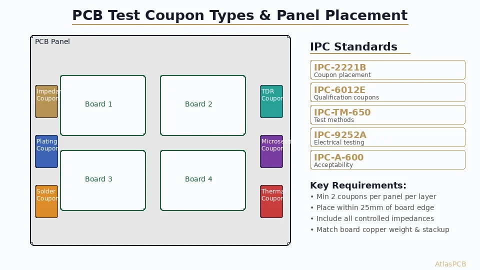
Coupon Placement
Coupons are placed in the panel border (rail area) or in waste areas between production boards. Key placement rules:
- Minimum one coupon per panel — IPC-6012 Class 3 requires impedance verification on every panel for controlled impedance layers
- Coupon must be on the same panel — not a separate test panel from a different production run
- Distribute coupons across the panel — at minimum, place coupons in two corners to detect panel-level etch variation
- Avoid panel edges — place coupons at least 10 mm from the panel edge to avoid edge effects in plating and etching
Trace Geometry Requirements
Each controlled impedance specification on the production board requires a corresponding coupon trace that replicates:
| Parameter | Must Match Production Board |
|---|---|
| Trace width | Identical nominal width |
| Copper weight (thickness) | Same layer, same copper weight |
| Dielectric thickness | Same prepreg/core between trace and reference plane |
| Reference plane | Same layer(s) used as ground/power reference |
| Solder mask coverage | If production traces are covered, coupon traces must be too |
| Trace-to-trace spacing (differential) | Identical for differential pairs |
Standard Coupon Structures
The following coupon types address the most common impedance requirements:
Single-ended microstrip (surface layer, no solder mask)
- Trace on outer layer, referenced to adjacent ground plane
- Used for validating high-speed single-ended signals on outer layers
Single-ended microstrip (with solder mask)
- Same as above but with solder mask applied
- Solder mask reduces impedance by 2–5 Ω due to increased effective dielectric constant
Single-ended stripline (inner layer)
- Trace on inner layer, sandwiched between two reference planes
- Used for validating inner-layer routing impedance
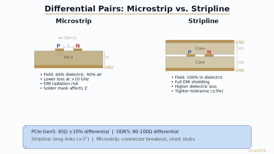
Differential microstrip
- Paired traces on outer layer with controlled spacing
- Common for USB, HDMI, PCIe, and other differential interfaces
Differential stripline
- Paired traces on inner layer between reference planes
- Common for high-speed serial links requiring maximum shielding
Broadside-coupled differential stripline
- Differential pair with traces on adjacent layers (one above the other)
- Used in dense routing where edge-coupled routing is impractical
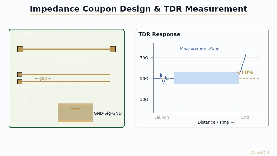
Coupon Dimensions
| Parameter | Recommended Value | Notes |
|---|---|---|
| Trace length | 150 mm (6 inches) minimum | Provides sufficient measurement window |
| Launch pad size | 0.5 mm × 0.75 mm (GS) or 0.5 mm × 0.5 mm (GSG) | Matches probe tip geometry |
| Launch pad-to-trace transition | Tapered over 0.5–1.0 mm | Minimizes launch discontinuity |
| Ground pad connection | Direct via to reference plane | ≤0.3 mm via diameter, ≤0.15 mm from pad edge |
| Trace-to-coupon-edge clearance | ≥5× dielectric thickness | Prevents edge coupling effects |
| Coupon width | ≥5 mm per trace structure | Allows clean probing access |
| End termination | Open (unterminated) | Standard for production TDR |
Launch Design
The launch structure—where the probe makes contact with the coupon—is the most critical element. A poorly designed launch introduces parasitic capacitance or inductance that distorts the impedance reading for the first several millimeters of trace.
Best practices for launch design:
- Use ground-signal (GS) or ground-signal-ground (GSG) pad configurations matching the TDR probe geometry
- Place ground vias immediately adjacent to the ground pad (within 0.15 mm) connecting to the reference plane
- Taper the trace width transition from launch pad to target trace width over 0.5–1.0 mm
- Remove solder mask from the launch area (even if production traces are solder-masked) for reliable probe contact
- Add anti-pad clearance around ground vias on non-reference layers to prevent parasitic coupling
- Use consistent launch designs across all coupons for measurement repeatability
For more detail on impedance specification in your design, refer to [how to specify impedance on PCB]/blog/how-to-specify-impedance-pcb/).
TDR Measurement Procedure
Equipment Setup and Calibration
Before measuring coupons, the TDR system must be calibrated:
- Warm-up: Allow the instrument 30–60 minutes to reach thermal equilibrium
- Cable compensation: Perform open/short/load calibration at the probe tip plane
- Rise time verification: Confirm the pulse rise time meets the specification (typically 35 ps for production testing)
- Impedance verification: Measure a known 50 Ω calibration standard; reading should be 50.0 ± 0.5 Ω
Measurement Process
- Position the probe on the coupon launch pads using a microscope or magnifying station
- Verify contact quality — the TDR trace should show a clean transition from the cable to the launch
- Set the measurement cursor to a stable region of the trace, excluding the first 3 mm (launch region) and the last 3 mm (end reflection region)
- Record the impedance value — the average impedance across the measurement region
- Measure at both ends — for differential pairs, measure from both launches and average
- Record ambient temperature — impedance varies approximately 0.05%/°C
Measurement Region Selection
The measurement region (also called the “gate” or “cursor window”) must exclude launch and termination artifacts:
| Region | Distance from Launch | Include in Measurement? |
|---|---|---|
| Launch transition | 0–3 mm | No — launch parasitics dominate |
| Stable trace region | 3 mm to (length – 3 mm) | Yes — this is the production-representative region |
| End reflection | Last 3 mm | No — open-circuit reflection distorts reading |
For a standard 150 mm coupon, the measurement region spans approximately 144 mm—providing an excellent statistical sample of the trace impedance.
Tolerance Analysis and Acceptance Criteria
Standard Impedance Tolerances
| Impedance Type | Standard Tolerance | Tight Tolerance | Premium Tolerance |
|---|---|---|---|
| Single-ended (outer layer) | ±10% | ±7% | ±5% |
| Single-ended (inner layer) | ±10% | ±7% | ±5% |
| Differential (outer layer) | ±10% | ±7% | ±5% |
| Differential (inner layer) | ±10% | ±7% | ±5% |
For a 50 Ω single-ended specification at ±10%, the acceptance range is 45.0–55.0 Ω. For the same specification at ±5%, the range narrows to 47.5–52.5 Ω.
Factors Affecting Impedance Variation
Understanding the sensitivity of impedance to each fabrication parameter is essential for process control. For a typical 50 Ω microstrip (5 mil trace, 4 mil dielectric, 1 oz copper on FR-4):
| Parameter | Typical Variation | Impedance Impact |
|---|---|---|
| Trace width | ±0.5 mil (±12.7 µm) | ±4–5 Ω (±8–10%) |
| Dielectric thickness | ±0.5 mil (±12.7 µm) | ±3–4 Ω (±6–8%) |
| Copper thickness | ±0.2 mil (±5 µm) | ±1–2 Ω (±2–4%) |
| Dielectric constant (Dk) | ±0.1 (from nominal 4.2) | ±1–2 Ω (±2–4%) |
| Solder mask thickness | ±0.3 mil (±7.6 µm) | ±0.5–1 Ω (±1–2%) |
Trace width is the dominant factor, which is why etch process control is the single most important determinant of impedance accuracy.
Root-Sum-Square (RSS) Analysis
Since fabrication variations are typically independent and normally distributed, the total impedance variation can be estimated using RSS:
For the parameters above, the RSS variation for a 50 Ω microstrip is approximately:
√(5² + 4² + 2² + 2² + 1²) ≈ ±7.1 Ω (±14.2%)
This explains why ±10% tolerance is the comfortable industry standard—it provides approximately 1.4σ margin for a well-controlled process. Tighter tolerances require reducing one or more variation sources, typically through:
- Laser direct imaging (LDI) for tighter etch control
- Controlled prepreg layup with measured dielectric thickness
- Premium laminate materials with tighter Dk tolerance
- Impedance-aware etch compensation
For differential pair-specific impedance considerations, see our guide on [impedance matching for differential pairs]/blog/pcb-impedance-matching-differential-pairs/).
Advanced Coupon Design Techniques
Multi-Impedance Coupons
Modern PCB designs often specify 4–8 different impedance values across multiple layers. Rather than creating individual coupons for each, multi-impedance coupons consolidate multiple trace structures into a single coupon strip:
- Arrange trace structures sequentially along the coupon length
- Separate each structure with a minimum 5 mm gap
- Provide individual launch pads for each structure
- Label each structure with its target impedance and layer
A well-designed multi-impedance coupon can validate 8–12 different impedance specifications in a 200 mm × 20 mm coupon area.
Embedded Coupon Verification
For critical applications (aerospace, medical, mil-spec), some designs include impedance verification structures directly on the production board, typically in areas that will be routed away or in connector footprint regions. These “embedded coupons” provide board-level verification that eliminates the panel-position variable.
Statistical Process Control (SPC) Coupons
For high-volume production, SPC coupons are measured on every panel and the results are trended over time. Key metrics to track:
| Metric | Purpose | Action Threshold |
|---|---|---|
| Mean impedance | Process centering | Target ± 3% |
| Standard deviation | Process variability | > 2% of target |
| Cpk | Process capability | < 1.33 |
| Trend (slope) | Process drift | > 0.5 Ω/week |
SPC analysis enables proactive process correction before impedance drifts out of specification—far better than reactive rejection of finished panels.
Common Coupon Design Mistakes
Mistake 1: Incorrect Reference Plane
The coupon trace must reference the same ground or power plane as the production trace. A common error is designing a coupon that references the adjacent plane rather than the actual reference plane used by the production trace. This is especially problematic in asymmetric stackups where inner layers have different dielectric thicknesses above and below.
Mistake 2: Missing Solder Mask on Microstrip Coupons
If the production microstrip traces are covered by solder mask (as they almost always are), the coupon traces must also be covered—except at the launch pads. Solder mask adds approximately 2–5 Ω to the impedance depending on mask thickness and Dk. Omitting it from the coupon creates a systematic measurement offset. Understanding [signal integrity design principles]/blog/signal-integrity-pcb-design-guide/) helps avoid these subtle errors.
Mistake 3: Insufficient Trace Length
Short coupons (<100 mm) do not provide enough measurement length after excluding launch and end regions. The result is a noisy measurement with poor averaging. Always design coupons ≥150 mm in trace length.
Mistake 4: Crosstalk Between Coupon Traces
Placing coupon traces too close together (especially differential pairs next to single-ended traces) introduces crosstalk that shifts the measured impedance. Maintain minimum 5× dielectric thickness spacing between independent coupon trace structures.
Mistake 5: Ground Via Starvation at Launch
Insufficient ground vias at the launch pad create an inductive discontinuity that appears as a high-impedance spike at the beginning of the TDR trace. This spike can be mistaken for a trace impedance issue. Use at minimum 2 ground vias per launch pad, placed within 0.15 mm of the pad edge.
Industry Standards for Impedance Testing
| Standard | Title | Key Requirements |
|---|---|---|
| IPC-2221B | Generic Standard on PCB Design | Defines impedance coupon requirements |
| IPC-TM-650 2.5.5.7 | Characteristic Impedance of Lines on PCBs by TDR | Defines TDR measurement methodology |
| IPC-6012E | Qualification and Performance Spec for Rigid PCBs | Impedance tolerance requirements by class |
| IPC-2141 | Design Guide for High-Speed Controlled Impedance Circuit Boards | Impedance design calculations |
| IPC-D-317 | Design Guidelines for Electronic Packaging Using High-Speed Techniques | Signal integrity and impedance guidelines |
IPC Class Requirements
| Requirement | Class 1 (General) | Class 2 (Dedicated) | Class 3 (High Reliability) |
|---|---|---|---|
| Impedance testing | If specified | If specified | Required for all impedance layers |
| Coupon per panel | Not required | Recommended | Required |
| Test records retention | 1 year | 5 years | Indefinite |
| SPC trending | Not required | Recommended | Required |
Practical Recommendations
For PCB Designers
- Specify impedance requirements clearly in your fabrication drawing—include target value, tolerance, and the specific nets/layers
- Include coupon areas in your panel design — allocate at least 20 mm width in the panel border for coupon structures
- Provide impedance stackup details — list the trace width, dielectric thickness, and reference plane for each impedance class
- Call out solder mask requirements — specify whether impedance is measured with or without solder mask
- Reference IPC standards — cite IPC-TM-650 2.5.5.7 for the measurement method
For PCB Fabricators
- Design coupons that match production exactly — verify trace width, copper weight, dielectric, and reference plane
- Calibrate TDR equipment daily — record calibration results in the quality system
- Control etch process tightly — invest in LDI and automated optical inspection (AOI) for trace width control
- Trend impedance data — implement SPC on every controlled impedance job
- Report actual measured values — not just pass/fail, provide the measured impedance for each coupon
Review [PCB testing methods]/blog/pcb-testing-methods/) for additional quality validation approaches beyond impedance measurement.
For Hardware Engineers
- Don’t over-specify tolerance — ±10% is sufficient for most applications including USB 3.x, PCIe Gen 4, DDR4, and HDMI 2.0
- Consider impedance budget — account for connector, via, and package impedance discontinuities alongside trace impedance
- Request impedance reports — every controlled impedance order should include TDR test data
- Validate first articles — for new designs, cross-check coupon measurements against 2D field solver predictions
- Plan for differential pairs — specify both odd-mode (single-ended equivalent) and differential impedance targets
Conclusion
Impedance test coupons are the quality gate between design intent and fabricated reality. A well-designed coupon program ensures that every production panel meets its controlled impedance specifications, preventing signal integrity failures that are expensive and time-consuming to debug in the lab.
The investment in proper coupon design—correct trace geometry, appropriate launch structures, adequate trace length, and systematic measurement procedures—pays dividends in first-pass yield, reduced debug time, and consistent electrical performance across production lots.
Whether your design requires standard ±10% tolerance on a 50 Ω microstrip or demanding ±5% tolerance on 100 Ω differential stripline, the principles in this guide will help you achieve reliable, repeatable impedance validation.
Upload your Gerbers for a free engineering review — our impedance engineering team will review your stackup, verify coupon designs, and ensure your controlled impedance specifications are achievable with our process capabilities.
Further Reading
- [PCB Rigid-Flex Bend Zone Reliability: Design Rules, Material Selection & Lifecycle Testing]/blog/pcb-rigid-flex-bend-zone-reliability/)
- [HDI PCB Design for 5G Antenna Integration: Signal Integrity Challenges in Millimeter-Wave Applications]/blog/hdi-5g-antenna-integration-pcb-design/)
- [ENEPIG vs ENIG Surface Finish: Complete Comparison for Wire Bonding, Solderability, and Long-Term Reliability]/blog/enepig-vs-enig-surface-finish-wire-bonding/)
- [PCB Surface Finish Comparison: OSP vs HASL vs Immersion Silver vs ENIG for Assembly Reliability]/blog/pcb-surface-finish-osp-hasl-enig-immersion-silver-comparison/)
- [Controlled Impedance PCB: Design, Stackup & Testing Explained]/blog/controlled-impedance-pcb/)
- Rigid PCB Manufacturing
About AtlasPCB — We specialize in complex PCB manufacturing for HDI, RF, and high-reliability applications. Explore our impedance-controlled PCB manufacturing . Every order includes free engineering review. Get your quote.
Reviewed by AtlasPCB Engineering Team — IPC-certified manufacturing specialists with 15+ years of production experience in HDI, RF, and high-reliability PCB fabrication. Content based on factory floor data and real customer design reviews.
- impedance-testing
- tdr
- test-coupon
- controlled-impedance
- signal-integrity