· AtlasPCB Engineering · Engineering · 7 min read
Stripline vs Microstrip: Choosing the Right Transmission Line for PCB Signal Routing
Compare stripline and microstrip transmission line geometries for PCB design. Understand impedance calculations, loss characteristics, EMI behavior, and when to use each topology for optimal signal integrity.
Transmission Line Fundamentals for PCB Engineers
Every PCB trace carrying signals with rise times faster than approximately one-sixth the propagation delay becomes a transmission line. At that point, the trace’s characteristic impedance — not just its DC resistance — determines signal behavior.
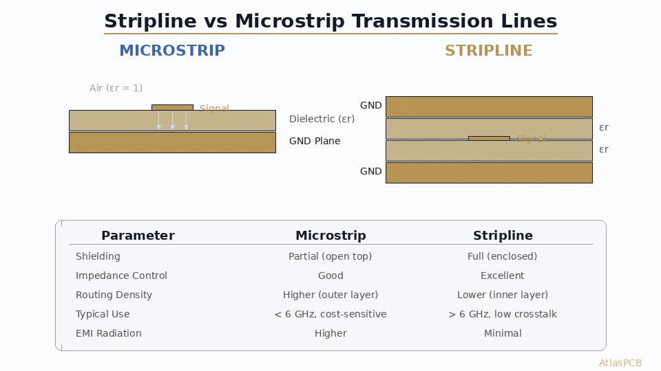
Two primary transmission line geometries dominate PCB design: microstrip (outer layer trace over a ground plane) and stripline (inner layer trace between two ground planes). Each has distinct electrical, thermal, and manufacturing characteristics that affect your design choices.
This guide provides the engineering analysis needed to make informed routing decisions for high-speed PCB designs.
Microstrip: Outer-Layer Routing
Geometry and Field Distribution
A microstrip trace sits on the outer surface of the PCB, with one ground reference plane below it separated by a dielectric layer. The electric field distribution is split between:
- Substrate dielectric (typically 60–70% of field energy): εr = 3.5–4.5 for FR-4
- Air above the trace (30–40% of field energy): εr = 1.0
This mixed dielectric creates an “effective dielectric constant” (εeff) that’s lower than the substrate’s actual εr:
$$\varepsilon_{eff} \approx \frac{\varepsilon_r + 1}{2} + \frac{\varepsilon_r - 1}{2} \cdot \frac{1}{\sqrt{1 + 12h/w}}$$
Where h = dielectric height, w = trace width.
For standard FR-4 (εr = 4.2) with h = 4 mil and w = 5 mil: εeff ≈ 3.1
Impedance Calculation
The characteristic impedance of a microstrip:
$$Z_0 = \frac{87}{\sqrt{\varepsilon_r + 1.41}} \cdot \ln\left(\frac{5.98h}{0.8w + t}\right) \quad \text{[ohms]}$$
Where:
- h = dielectric thickness
- w = trace width
- t = copper thickness
- Valid for w/h ratio between 0.1 and 3.0
Typical 50Ω microstrip dimensions (FR-4, 1 oz copper):
- 4 mil trace over 3.5 mil dielectric
- 5 mil trace over 4.2 mil dielectric
- 8 mil trace over 7 mil dielectric
Advantages of Microstrip
- Lower insertion loss — air portion of the field has zero dielectric loss
- Easier impedance tuning — outer layer allows post-fab measurement and trimming
- Better heat dissipation — exposed copper radiates heat directly
- Component access — traces on outer layers connect directly to SMT pads
- Lower cost — fewer layers needed for signal routing
Disadvantages of Microstrip
- EMI radiation — open field structure acts as an antenna
- Environmental sensitivity — conformal coating or solder mask changes εeff
- Crosstalk — unshielded fields couple more easily to adjacent traces
- Dispersion — εeff varies with frequency due to field redistribution
- Solder mask impact — additional dielectric layer (εr ≈ 3.3) alters impedance by 2–5 Ω
Stripline: Inner-Layer Routing
Geometry and Field Distribution
A stripline trace is embedded between two ground planes, with the entire electric field contained within a uniform dielectric medium. This creates a true TEM (Transverse Electromagnetic Mode) propagation with:
- No fringing fields in air
- Constant εeff = εr of the substrate material
- Complete electromagnetic shielding by the ground planes
Symmetric vs. Asymmetric Stripline
Symmetric (centered) stripline: Equal dielectric thickness above and below the trace. This is the ideal geometry for impedance control.
Asymmetric (offset) stripline: Trace closer to one ground plane than the other. Common in practical stackups where routing layers don’t fall exactly at the midpoint. The impedance calculation requires the “dual dielectric” formula:
$$Z_0 \approx \frac{60}{\sqrt{\varepsilon_r}} \cdot \ln\left(\frac{4b}{\pi \cdot 0.67 \cdot (0.8w + t)}\right) \quad \text{[symmetric]}$$
Where b = total distance between ground planes.
For asymmetric stripline, use field-solver tools (e.g., Polar Si9000) for accurate results.
Impedance Calculation
Typical 50Ω stripline dimensions (FR-4, 1 oz copper):
- 4 mil trace between ground planes 12 mil apart (symmetric)
- 3.5 mil trace between ground planes 10 mil apart
- 5 mil trace between ground planes 14 mil apart
Advantages of Stripline
- Superior EMI containment — fields fully shielded between ground planes
- Excellent crosstalk isolation — ground planes prevent inter-layer coupling
- Consistent impedance — no environmental or coating sensitivity
- No dispersion — pure TEM mode means εeff is frequency-independent
- Better for differential pairs — tight coupling control with consistent geometry
Disadvantages of Stripline
- Higher insertion loss — entire field passes through lossy dielectric
- No direct component access — requires vias for layer transitions
- Reduced routing density — ground planes consume layers
- Tighter manufacturing tolerance — inner layer registration affects impedance
- Via transitions required — every layer change introduces discontinuity

Need Impedance-Controlled PCBs?
AtlasPCB delivers ±5% impedance tolerance with TDR verification on every controlled-impedance lot.
Get a Quote →Loss Comparison: The Critical Engineering Trade-off
Dielectric Loss (α_d)
Dielectric loss dominates above ~2 GHz and scales linearly with frequency:
$$\alpha_d = \frac{\pi f \sqrt{\varepsilon_{eff}}}{c} \cdot \tan\delta \quad \text{[Np/m]}$$
For microstrip, only ~65% of the field energy passes through the dielectric, reducing effective tanδ:
$$\tan\delta_{eff,microstrip} \approx 0.65 \cdot \tan\delta_{substrate}$$
For stripline, 100% passes through the dielectric:
$$\tan\delta_{eff,stripline} = \tan\delta_{substrate}$$
Practical example at 10 GHz (standard FR-4, tanδ = 0.020):
- Microstrip loss contribution: ~0.45 dB/inch
- Stripline loss contribution: ~0.70 dB/inch
This 55% higher dielectric loss for stripline is the primary reason high-speed designs often select low-loss laminates like Megtron 6 (tanδ = 0.004) or Rogers 4350B (tanδ = 0.0037) for stripline layers.
Conductor Loss (α_c)
Conductor loss depends on skin effect resistance and scales with √f:
$$\alpha_c = \frac{R_s}{Z_0 \cdot w_{eff}} \quad \text{[Np/m]}$$
The difference between microstrip and stripline conductor loss is small (5–15%) for the same trace width, but stripline typically uses narrower traces for the same Z0, increasing conductor loss slightly.
Total Loss Budget
For a 6-inch channel at 25 Gbps (PCIe Gen5 fundamental at 12.5 GHz):
| Parameter | Microstrip (Meg6) | Stripline (Meg6) |
|---|---|---|
| Dielectric loss | 0.55 dB/in | 0.85 dB/in |
| Conductor loss | 0.35 dB/in | 0.40 dB/in |
| Total/inch | 0.90 dB/in | 1.25 dB/in |
| 6-inch channel | 5.4 dB | 7.5 dB |
This 2.1 dB difference matters significantly when the channel loss budget is tight (PCIe Gen5 allows ~20 dB at Nyquist for the full channel including connectors and vias).
Design Decision Framework
Use Microstrip When:
- Frequency < 6 GHz and EMI is manageable with other techniques
- Board layer count is constrained (cost optimization)
- Test point access is needed for production verification
- Thermal dissipation from high-power traces is a concern
- First prototype and impedance may need tuning
- Component-dense outer layers need direct routing
Use Stripline When:
- Operating frequency > 6 GHz
- EMI compliance is critical (FCC/CISPR class B)
- Differential pairs require < 5% intra-pair skew
- Military/aerospace per MIL-STD-461 radiated emissions
- Clock distribution networks need low jitter
- Dense routing with tight crosstalk budget
- Mixed-signal isolation between analog and digital domains
Hybrid Approach (Most Common)
Modern 8–16 layer PCBs typically use both:
- Outer layers (microstrip): Power delivery, low-speed I/O, test points, LED signals
- Inner layers (stripline): High-speed SerDes, DDR5 data, clock networks, RF traces
The critical challenge becomes managing the via transition between microstrip and stripline sections.
Via Transitions Between Geometries
Every signal that moves from an outer-layer microstrip to an inner-layer stripline passes through a via — creating an impedance discontinuity. The via’s parasitic inductance (typically 0.5–1.5 nH for a standard through-hole via) and capacitance (0.3–0.8 pF) create reflections at multi-GHz frequencies.
Mitigation strategies:
- Back-drilling to remove via stubs
- Anti-pad optimization to control via capacitance
- Ground via stitching around signal vias for return path continuity
- Blind/buried vias to minimize stub length from the start
For signals above 16 Gbps, via modeling in a 3D field solver becomes mandatory to achieve target channel performance.
Manufacturing Considerations
Impedance Tolerance
| Parameter | Microstrip | Stripline |
|---|---|---|
| Typical tolerance | ±7–10% | ±8–10% |
| Best achievable | ±5% | ±5% |
| Critical process | Etch, dielectric thickness | Registration, dielectric thickness |
| Main variation source | Etch undercut (trace width) | Prepreg pressing (thickness) |
Process Compensation
For microstrip:
- Apply etch compensation to maintain target trace width
- Account for solder mask impedance impact in simulation
- Specify copper roughness profile (HVLP preferred for > 5 GHz)
For stripline:
- Specify prepreg press-out tolerance
- Control resin content variation between prepreg sheets
- Verify inner layer registration accuracy
Further Reading
- S-Parameter Analysis for PCB Interconnects
- Copper Roughness and High-Speed Signal Loss
- Differential Impedance for PCIe Gen5 and DDR5
- RF PCB Material Selection Guide
Building high-speed boards that mix microstrip and stripline? AtlasPCB provides stackup optimization, impedance simulation, and TDR verification as part of our engineering review service. Get a quote for your next impedance-controlled design.
About AtlasPCB — We specialize in complex PCB manufacturing for HDI, RF, and high-reliability applications. Explore our RF and high-frequency PCB services, or get an impedance-controlled PCB manufacturing . Every order includes free engineering review. Get your quote.
Reviewed by AtlasPCB Engineering Team — IPC-certified manufacturing specialists with 15+ years of production experience in HDI, RF, and high-reliability PCB fabrication. Content based on factory floor data and real customer design reviews.
- stripline
- microstrip
- transmission-line
- signal-integrity
- impedance
- pcb-design
- rf
- high-speed