· AtlasPCB Engineering · Engineering · 8 min read
PCB ESD Protection Design: TVS Selection, Guard Ring Layout, and IEC 61000-4-2 Compliance
Complete guide to PCB-level ESD protection design. Learn TVS diode selection, guard ring layout, trace routing rules, and testing methods per IEC 61000-4-2 and IPC standards for robust electronics.
The Physics of ESD Damage on PCBs
Electrostatic discharge is one of the most common and least visible causes of electronic product failures. A human body charged to 8,000 V can deliver a current pulse exceeding 30 A peak with a rise time under 1 nanosecond — faster than most semiconductor junctions can absorb without damage. The energy is small (microjoules), but the instantaneous power density at the point of discharge can exceed the damage threshold of gate oxides, thin-film resistors, and even copper traces.
ESD damage manifests in two ways:
- Hard failure — Immediate destruction of a gate oxide, junction, or trace. The IC stops working.
- Latent damage — Partial degradation that weakens the device without causing immediate failure. The product passes testing but fails prematurely in the field. This is more insidious because it is invisible to standard quality screens.
Effective ESD protection is not optional — it is a design requirement for every product that will be handled by humans, installed in an uncontrolled environment, or connected to external cables.

IEC 61000-4-2: The Standard That Defines the Threat
The international standard IEC 61000-4-2 defines the ESD test methodology and severity levels that products must withstand:
Test Levels
| Level | Contact Discharge | Air Discharge |
|---|---|---|
| 1 | ±2 kV | ±2 kV |
| 2 | ±4 kV | ±4 kV |
| 3 | ±6 kV | ±8 kV |
| 4 | ±8 kV | ±15 kV |
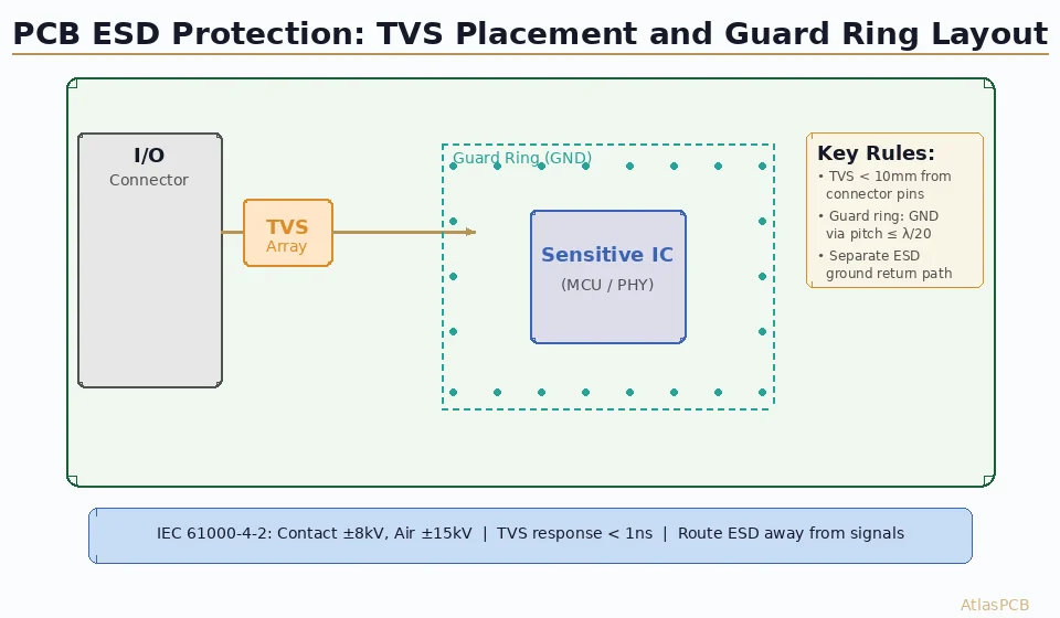
Most commercial products target Level 4 (±8 kV contact, ±15 kV air). Automotive and industrial products may require higher levels per their own standards (ISO 10605 for automotive specifies up to ±25 kV air discharge).
The ESD Current Waveform
The IEC 61000-4-2 discharge waveform has two critical components:
- Initial spike: 0.7–1 ns rise time, ~3.75 A/kV peak current. At ±8 kV, this is 30 A peak in under 1 ns. This component causes gate oxide damage and trace coupling.
- Bulk discharge: ~30 ns to peak of the slower human-body component, ~1.875 A/kV. This sustains the energy transfer and causes thermal damage.
The combination means your protection circuit must respond in sub-nanosecond time and handle both the transient power of the initial spike and the sustained energy of the bulk discharge.
Component-Level Protection: TVS Diode Selection
Operating Principle
A TVS (Transient Voltage Suppressor) diode is a specialized Zener-type device optimized for absorbing fast transient energy. In normal operation, it appears as a high-impedance element (essentially invisible to the circuit). When the voltage exceeds its breakdown threshold, it clamps rapidly, diverting the transient current to ground.
For ESD protection specifically, look for:
- Response time: < 1 ns (semiconductor-based TVS is inherently fast)
- Low clamping voltage: V_clamp at peak pulse current must be below IC damage threshold
- Low capacitance: < 1 pF for high-speed data lines (USB 3.x, HDMI 2.1, Ethernet)
- Low leakage: < 1 µA at working voltage to avoid affecting signal integrity
TVS Selection Flowchart
Determine working voltage — What is the normal signal voltage range? Select TVS standoff voltage (V_RWM) > maximum signal voltage including tolerance.
Determine IC damage threshold — What is the protected IC’s absolute maximum voltage on that pin? This is your ceiling.
Select TVS clamping voltage — V_clamp at the expected peak pulse current (typically 16A for ±8kV contact discharge) must be < IC abs max voltage. Leave ≥ 0.5V margin.
Check capacitance — For data rates above 1 Gbps, TVS capacitance must be < 1 pF (ideally < 0.5 pF). For USB 2.0 (480 Mbps), up to 5 pF is acceptable.
Check package and footprint — ESD TVS arrays come in ultra-small packages (0201, SOD-882). Smaller packages enable closer placement to connector pins.
TVS Arrays for Common Interfaces
| Interface | Working Voltage | Max TVS Cap | Recommended TVS Family |
|---|---|---|---|
| USB 2.0 | 5V | 5 pF | Unidirectional, V_clamp < 12V |
| USB 3.x / USB4 | 3.3V | 0.5 pF | Low-cap array, V_clamp < 5.5V |
| HDMI 2.1 | 3.3V | 0.3 pF | Ultra-low-cap, V_clamp < 6V |
| Ethernet (PHY) | 3.3V | 3 pF | Multi-channel array |
| GPIO (3.3V) | 3.3V | 5 pF | Standard TVS, V_clamp < 6V |
| Automotive CAN | 5V | 15 pF | Bidirectional, V_clamp < 24V |
Bidirectional vs. Unidirectional
- Unidirectional TVS: Clamps in one polarity only. Use for signals with a DC bias or signals that should never go negative (most digital interfaces).
- Bidirectional TVS: Clamps symmetrically in both polarities. Use for signals that swing positive and negative (RS-485, analog signals, audio).
Designing Products That Must Pass ESD Testing?
AtlasPCB fabricates boards with integrated guard ring structures and controlled impedance for EMC-sensitive designs. Get expert DFM review included.
Get a Quote →Board-Level Protection: Layout Techniques
TVS Placement Rules
The number one layout mistake is placing the TVS diode far from the connector or on a trace stub. The ESD pulse rise time is under 1 ns — at 3×10⁸ m/s in free space (and roughly half that in PCB traces), 1 ns corresponds to ~75 mm of trace length. Any inductance between the ESD entry point and the TVS allows the full voltage spike to pass.
Critical rules:
Distance: TVS pads must be within 10 mm of the connector pin. Ideally, place the TVS between the connector and the first routing layer change (via).
In-line routing: Route the signal FROM connector pin → TO TVS pad → FROM TVS pad → TO IC. Never route the signal past the TVS and branch back to it.
Ground return path: The TVS ground pin must connect to the nearest ground plane via on the shortest possible path (< 5 mm trace to via). A long ground return adds inductance that raises the effective clamping voltage.
Dedicated ground vias: Use at least 2 ground vias per TVS array to reduce ground return inductance. For multi-channel TVS arrays (4+ channels), use 3–4 ground vias.
Separate ESD ground zone: For the highest immunity, create a dedicated ESD ground area near the connectors that connects to the main ground plane through a controlled path. This prevents ESD ground currents from coupling into sensitive signal ground.
Guard Ring Design
A guard ring is a grounded copper trace on the surface layer that surrounds the protected circuit area. It intercepts surface-coupled ESD energy and provides a low-impedance path to ground.
Guard ring specifications:
- Trace width: ≥ 0.5 mm (20 mil) — wider is better for low impedance
- Layer: Top and bottom surface layers where ESD coupling is strongest
- Via spacing: ≤ 5 mm (for ESD frequencies up to 300 MHz). Calculate as λ/20 of the highest frequency of concern.
- Via size: 0.3 mm drill, standard plated through-hole
- Connection: Tied to chassis ground or signal ground depending on grounding architecture
- Gap management: Any gap in the guard ring (for signal routing in/out of the protected zone) must be as narrow as possible (< 1 mm) and bridged on an inner layer
Trace Routing for ESD Immunity
Do:
- Keep ESD-exposed traces (from connectors to TVS) on surface layers where they can be guard-ring protected
- Use short, wide traces for ESD paths
- Provide continuous ground planes under ESD-sensitive areas
- Route sensitive signals perpendicular to ESD-exposed traces (minimize coupling length)
- Use [ground plane stitching vias]/blog/pcb-ground-plane-stitching-via/) around connector areas
Don’t:
- Route ESD-exposed traces as microstrips over split ground planes
- Run sensitive traces parallel to and adjacent to connector traces
- Use via stubs on ESD ground returns (see [back drilling]/blog/pcb-back-drilling-via-stub-removal-signal-integrity/))
- Leave floating copper near discharge points (it couples and re-radiates)
Testing and Compliance
Pre-Compliance ESD Testing
Before sending a product for formal certification, perform pre-compliance ESD testing:
- Setup: ESD simulator (IEC-compliant gun), horizontal/vertical coupling planes per IEC 61000-4-2
- Test points: All accessible metal surfaces, connector pins, seams, buttons, display edges
- Criteria:
- Performance Criteria A: No degradation during or after test
- Performance Criteria B: Temporary loss of function during test, self-recovers
- Performance Criteria C: Temporary loss requiring operator intervention
- Unacceptable: Permanent damage or data loss
Debugging ESD Failures
When a product fails ESD testing, systematic debugging identifies the weak point:
- Identify the discharge path: Where is current flowing? Use a near-field EMI probe to trace the ESD energy.
- Check TVS response: Monitor the clamped voltage with a high-bandwidth oscilloscope (≥ 2 GHz). Is the TVS clamping below the IC damage threshold?
- Check ground return: Measure voltage drop across the TVS ground path. High impedance here raises effective clamping voltage.
- Check coupling: Are long traces acting as antennas, coupling ESD energy into circuits that are not directly connected to the discharge point?
PCB-Level Improvements for Failed Products
If a product fails ESD testing and a board redesign is needed:
- Add or resize guard rings
- Move TVS closer to connector
- Add ground stitching vias around the failing connector
- Widen ground return traces from TVS to ground plane
- Add a ground plane copper fill on an inner layer under the connector area if one does not exist
- Consider adding a ferrite bead between the connector and TVS for additional high-frequency filtering (but ensure it does not slow the TVS response)
Design Checklist
✅ TVS diode selected with V_clamp < IC abs max voltage (≥ 0.5V margin) ✅ TVS placed within 10 mm of connector pins, in-line with signal routing ✅ TVS ground return: ≤ 5 mm to ground plane via, with ≥ 2 dedicated ground vias ✅ Guard ring surrounds sensitive circuitry, via spacing ≤ 5 mm ✅ No ground plane splits under ESD-exposed traces ✅ Sensitive signals routed perpendicular to ESD-exposed traces ✅ ESD-exposed traces on surface layers (guard-ring protected) ✅ Fabrication notes specify controlled impedance for high-speed ESD-protected interfaces ✅ [PCB stackup]/blog/pcb-stackup-design-guide/) provides continuous ground reference under all signal layers ✅ Pre-compliance ESD testing planned before formal certification
Further Reading
- [PCB Ground Plane Stitching Vias]/blog/pcb-ground-plane-stitching-via/)
- [PCB Grounding Techniques: Star, Split, and Solid Strategies]/blog/pcb-grounding-techniques/)
- [PCB Design for EMI Compliance]/blog/pcb-design-emi-compliance/)
- [Controlled Impedance PCB Stackup Design]/blog/controlled-impedance-pcb-design-stackup-calculations/)
- [PCB Stackup Design Guide]/blog/pcb-stackup-design-guide/)
Need PCBs designed for ESD compliance? Contact AtlasPCB for boards with integrated guard ring structures, controlled impedance, and full DFM review. We help hardware teams pass ESD certification on the first attempt.
About AtlasPCB — We specialize in complex PCB manufacturing for HDI, RF, and high-reliability applications. Explore our full PCB manufacturing capabilities, or get an instant online quote . Every order includes free engineering review. Get your quote.
Reviewed by AtlasPCB Engineering Team — IPC-certified manufacturing specialists with 15+ years of production experience in HDI, RF, and high-reliability PCB fabrication. Content based on factory floor data and real customer design reviews.
- esd-protection
- pcb-design
- tvs-diode
- emc
- reliability
- layout-design