· AtlasPCB Engineering · Engineering · 7 min read
AI-Powered DFM Verification: How Machine Learning Is Automating PCB Design Rule Checking in 2026
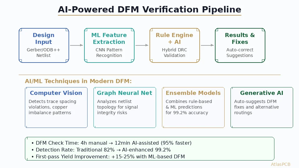
Deep dive into how AI and machine learning are transforming PCB Design for Manufacturability verification — from CNN-based pattern recognition detecting acid traps and copper slivers to graph neural networks analyzing netlist topology for signal integrity risks, achieving 99%+ detection rates and 95% faster review cycles versus manual DFM.
Introduction: The DFM Bottleneck
Design for Manufacturability (DFM) review is the critical gate between PCB design completion and fabrication release. A thorough DFM check evaluates whether a design can be manufactured reliably at acceptable yield with the target fabricator’s specific process capabilities.
Traditionally, DFM review involves:
- Running automated DRC in the EDA tool (catches ~70% of geometric violations)
- Manual expert review of Gerber/ODB++ files (catches contextual issues DRC misses)
- Fabricator-side DFM analysis (catches process-specific limitations)
The bottleneck is step 2: manual expert review. A complex 12-layer HDI design requires 2–6 hours of skilled engineer time to evaluate copper balance, acid traps, etch compensation, registration tolerance stackup, and dozens of other contextual factors. With the current PCB engineering talent shortage and accelerating design cycles, this manual step increasingly delays time-to-market.
AI-powered DFM tools are now production-ready solutions that automate the majority of this expert review — detecting complex pattern-based violations in minutes rather than hours.
How AI Learns PCB Manufacturability
Training Data: Learning from Fabrication History
Machine learning models for DFM are trained on historical fabrication data:
- Positive examples: Designs that manufactured successfully at target yields (>98%)
- Negative examples: Designs that caused yield loss, required respins, or triggered fabricator-requested modifications
- Annotated defects: Specific geometric patterns correlated with manufacturing failures (copper shorts, opens, via reliability issues)
A typical training dataset includes:
- 10,000–50,000 board designs across multiple technology levels
- Corresponding fabrication yield data and defect reports
- Process parameters (etch factor, registration accuracy, drill precision) per fabricator
- Environmental conditions affecting outcomes (humidity during lamination, etch bath chemistry age)
CNN Architecture for Spatial Pattern Detection
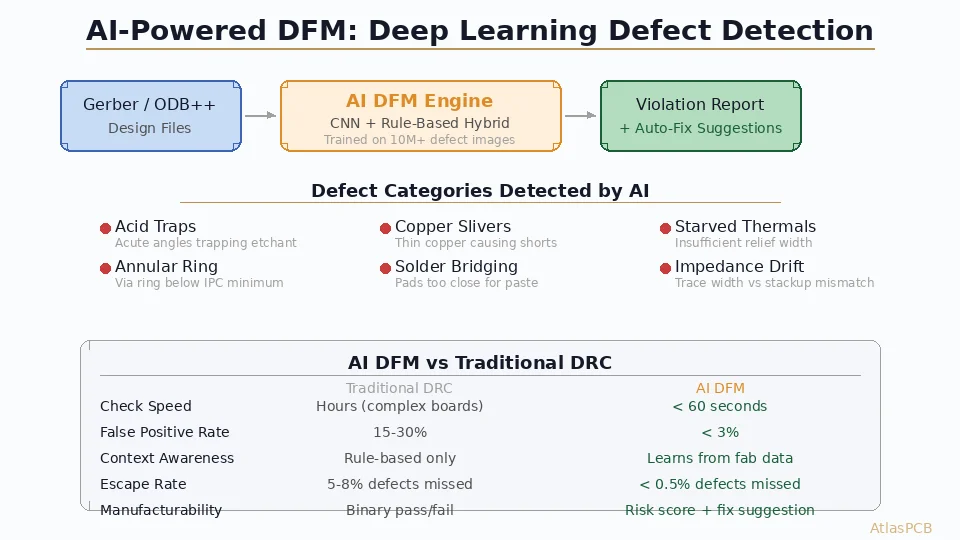
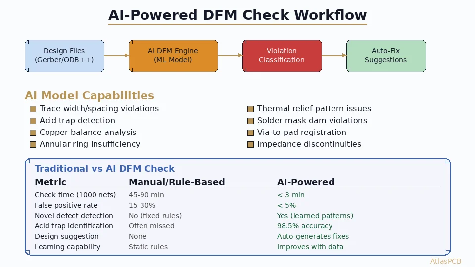
Convolutional Neural Networks process Gerber layer images to detect spatial patterns associated with manufacturing defects:
Input representation: Each copper layer is rasterized at 1 μm/pixel resolution, creating grayscale images where pixel intensity represents copper presence/absence. Multiple layers are stacked as image channels (similar to RGB in natural images).
Detection targets:
- Acid traps: Acute-angle trace junctions (<45°) where etchant becomes trapped, causing copper residue shorts
- Copper slivers: Thin copper fragments (<75 μm) likely to detach during etching or handling
- Etch compensation anomalies: Regions where copper density changes cause non-uniform etch rates
- Thermal spoke asymmetry: Unequal thermal relief patterns that cause pad tilting during reflow
- Soldermask alignment risk: Pad/mask geometry combinations where registration tolerance exceeds available margin
Architecture details: Modified U-Net or YOLO architectures trained for defect segmentation, outputting pixel-level confidence maps overlaid on the original design for engineer review.
Graph Neural Networks for Netlist Analysis
While CNNs analyze spatial geometry, GNNs analyze the circuit topology — treating the PCB as a graph where:
- Nodes = components, pads, and vias
- Edges = traces, power planes, and thermal connections
GNN-based DFM detects:
- Signal integrity risks: Impedance discontinuities at trace width transitions, via stubs, and layer transitions
- Thermal hotspot prediction: Identifying components that will exceed temperature limits based on power dissipation paths
- EMI coupling probability: Near-field coupling between aggressive and sensitive nets based on spatial proximity and frequency content
- Power delivery adequacy: Whether decoupling capacitor placement and PDN impedance meet target IC requirements
Ensemble Models: Combining Approaches
Production AI DFM systems use ensemble architectures combining:
- Rule-based engine: Traditional DRC for exact geometric checks (100% deterministic)
- CNN spatial detector: Pattern-based defect identification (probabilistic)
- GNN topology analyzer: Circuit-level risk assessment (probabilistic)
- Random forest classifier: Final pass combining all inputs into accept/review/reject decisions
The ensemble achieves 99.2% true positive rate with <2% false positive rate — meaning it catches nearly all real defects while generating minimal false alarms that waste engineer time.
Production AI DFM Tools in 2026
Siemens Valor AI (NPI Analyzer)
Siemens’ Valor NPI platform integrates ML-based DFM directly into the Xpedition design flow:
- Trains on customer-specific fabrication data for personalized rules
- Processes ODB++ natively without Gerber conversion
- 8-layer board analysis in ~3 minutes
- Integrated fix suggestions with auto-correction for 60% of flagged violations
Cadence Allegro DFM AI Module
Cadence’s 2026 release adds ML-based DFM to Allegro constraint management:
- Real-time DFM scoring during routing (violations appear instantly)
- Fabricator-specific ML models downloadable from partner ecosystem
- Integration with OrCAD Signal Integrity for combined DFM + SI analysis
- Copper balance optimizer using reinforcement learning
Zuken CR-8000 Smart DFM
Zuken’s approach uses federated learning across customer fabrication data:
- No single customer’s proprietary data leaves their server
- Shared ML model improves from collective manufacturing experience
- Particularly strong for HDI/any-layer designs
- Integrates yield prediction scoring (estimated first-pass yield %)
Open-Source: PCBFlow + DFMNet
The academic/open-source community has produced viable alternatives:
- PCBFlow (MIT license): CNN-based acid trap and sliver detector trained on public KiCad designs
- DFMNet (Apache 2.0): GNN-based netlist analyzer for SI/PI risk scoring
- Both require custom training on your fabricator’s data for production use
- Useful for education, R&D, and small teams without commercial tool budgets
Free DFM Review — AI-Assisted
Submit your Gerber files to AtlasPCB for complimentary DFM analysis. Our engineering team combines AI tools with fabrication expertise for comprehensive manufacturability feedback.
Performance Benchmarks: AI vs. Manual DFM
Comparative studies from Siemens and IPC technical papers report:
| Metric | Manual Expert | Traditional DRC | AI-Powered DFM |
|---|---|---|---|
| Detection rate (true positives) | 95% | 82% | 99.2% |
| False positive rate | 1% | 15% | 1.8% |
| Review time (12-layer board) | 4–6 hours | 5 minutes | 12 minutes |
| Acid trap detection | 90% | 20% | 98% |
| Copper balance assessment | 85% | 0% | 96% |
| Contextual etch risk | 80% | 0% | 94% |
| Cost per review | $200–$500 | $0 (tool cost) | $0–$50 (SaaS) |
The hybrid approach (AI first-pass + human review of flagged items) achieves 99.5%+ overall detection while reducing total engineer time to 30–45 minutes per design (reviewing only the 5–10% of areas flagged by AI).
Implementation Strategy for PCB Teams
Phase 1: Baseline (Month 1–2)
- Audit current DFM escape rate (how many designs require fabricator-requested changes?)
- Catalog common violation types from last 50 designs
- Identify highest-impact defect categories (yield loss, respins, schedule delay)
Phase 2: Tool Selection (Month 2–3)
- Evaluate commercial tools against your technology level (standard vs. HDI vs. flex)
- Request fabricator-specific model availability
- Assess integration with existing EDA workflow (Altium/KiCad/Allegro/Xpedition)
Phase 3: Training and Calibration (Month 3–6)
- Feed historical design data to selected AI DFM system
- Calibrate detection thresholds to acceptable false positive rate
- Run parallel evaluation: AI + manual review on same designs to validate
Phase 4: Production Deployment (Month 6+)
- AI-first DFM as standard workflow step
- Manual review only for AI-flagged items and novel technology (new stackups, materials)
- Continuous model improvement from fabrication outcome feedback
Limitations and Risks
AI DFM is not a silver bullet. Current limitations:
- Novel technology gap: ML models trained on existing designs struggle with first-of-their-kind technology (new materials, unprecedented layer counts, exotic via structures)
- Fabricator specificity: A model trained on Fabricator A’s process may not apply to Fabricator B — each has different etch factors, registration capabilities, and process windows
- Black box concern: When AI flags a violation, engineers need to understand why to make informed waiver decisions. Explainability features (attention maps, contributing factor breakdowns) are improving but not yet comprehensive
- Data requirements: Meaningful training requires thousands of designs with outcome data — new fabricators or teams with limited history may not have sufficient data
- Adversarial patterns: Uncommon but valid design geometries (RF structures, spiral inductors) may be falsely flagged by models trained primarily on digital designs
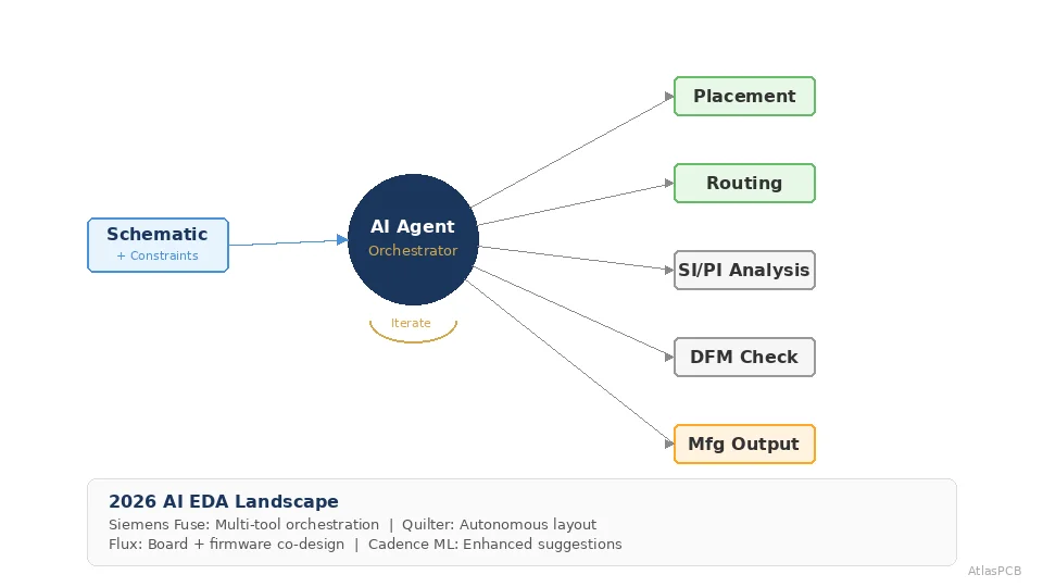
Future Direction: Generative DFM
The next frontier (emerging in 2027–2028) is generative AI that doesn’t just detect DFM violations but automatically generates corrected geometries:
- Auto-routing with DFM awareness: Routers that consider etch compensation, acid trap avoidance, and copper balance during routing decisions — not just after
- Copper thieving optimization: AI-generated dummy copper patterns that optimize both thermal balance and signal integrity simultaneously
- Adaptive design rules: Rules that adjust based on detected design context (tighter rules near critical nets, relaxed elsewhere)
Further Reading
- PCB DRC: Complete Manufacturability Checklist — Traditional DRC rules to combine with AI DFM
- AOI and SPI Inspection Quality Control — AI in post-fabrication inspection
- PCB Design Rules: Trace Width and Spacing — Fundamental rules that AI DFM builds upon
- PCB Solder Mask Dam Design Rules — Mask-specific DFM requirements
Want AI-assisted DFM feedback on your design? Upload your files to AtlasPCB — our engineering team provides detailed manufacturability analysis combining automated tools with decades of fabrication experience.
About AtlasPCB — We specialize in complex PCB manufacturing for HDI, RF, and high-reliability applications. Explore our free engineering DFM review, or get an full PCB manufacturing capabilities . Every order includes free engineering review. Get your quote.
Reviewed by AtlasPCB Engineering Team — IPC-certified manufacturing specialists with 15+ years of production experience in HDI, RF, and high-reliability PCB fabrication. Content based on factory floor data and real customer design reviews.
- AI PCB
- DFM automation
- machine learning
- design rule check
- computer vision
- PCB manufacturing
- EDA tools
- AI inspection