· AtlasPCB Engineering · Engineering · 7 min read
Tin Whisker Growth on PCBs: Risk Assessment, Mechanisms, and Mitigation Strategies
Engineering guide to tin whisker formation on PCB surface finishes and component leads. Covers growth mechanisms, risk factors, JEDEC JEIP39 testing, conformal coating mitigation, and surface finish alternatives for high-reliability electronics.
The Silent Threat: Tin Whiskers in Modern Electronics
In 2005, a European communications satellite suffered a catastrophic power bus short caused by a conductive filament only 4µm in diameter. In 2002, a nuclear reactor’s safety monitoring system experienced unexplained intermittent faults traced to metallic bridges between component leads spaced 0.5mm apart. These incidents share a common root cause: tin whiskers.
Tin whiskers are single-crystal metallic filaments that grow spontaneously from tin-plated surfaces without any external electrical field or intentional process. They represent one of the most insidious reliability threats in electronics because:
- They grow slowly and unpredictably over months to decades
- They’re invisible to the naked eye (1-10µm diameter)
- They can bridge conductors up to 10mm apart
- They carry enough current to cause permanent shorts or transient arcing
- No screening test reliably detects whisker-prone assemblies before deployment
The transition to lead-free (RoHS) electronics in 2006 dramatically amplified this risk. The 1-3% lead content historically added to tin plating inhibited whisker growth; its removal created a generation of electronics with unprecedented whisker susceptibility.

Growth Mechanisms and Physics
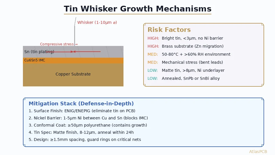
Compressive Stress: The Driving Force
Tin whiskers are a stress relief mechanism. When compressive stress accumulates within a polycrystalline tin film, the crystal lattice stores elastic energy. If the stress exceeds a threshold (~8-10 MPa for pure tin), individual grains can nucleate whisker growth as a mechanism to relieve that stored energy.
The whisker grows from its base (not the tip), with atoms diffusing along grain boundaries toward the whisker root. A single grain acts as the nucleation site, and the emerging filament is typically a single crystal with a preferred <001> growth direction.
Primary Stress Sources
1. Intermetallic Formation (Cu6Sn5 / Cu3Sn)
When tin is deposited directly on copper (the most common PCB scenario), copper atoms diffuse into the tin layer and form Cu6Sn5 intermetallic compound (IMC) at the interface. This reaction:
- Consumes tin at the interface, creating compressive stress in the remaining tin
- Produces IMC with ~40% volume expansion compared to pure copper
- Continues at room temperature, albeit slowly (diffusion-controlled)
- Accelerates at elevated temperatures (50-80°C is the worst-case range)
2. Mechanical Stress
External forces applied during:
- Lead forming and bending operations
- Connector insertion/extraction
- Press-fit contacts
- PCB flexure in service
- Clamping force from heatsinks or fasteners
3. Thermal Cycling Stress
The coefficient of thermal expansion (CTE) mismatch between tin (~22 ppm/°C) and the underlying copper (~17 ppm/°C) or iron (~12 ppm/°C for Alloy 42 lead frames) generates cyclic compressive/tensile stress during temperature excursions.
4. Corrosion-Induced Stress
In humid environments with contamination (flux residue, sulfur compounds), localized corrosion produces oxide and hydroxide products at grain boundaries. These corrosion products occupy more volume than the parent metal, creating compressive stress that nucleates whiskers.
Environmental Acceleration Factors
| Factor | Effect on Whisker Growth |
|---|---|
| Temperature 50-80°C | Maximum growth rate (IMC kinetics + stress) |
| Humidity >60% RH | Accelerates corrosion-driven whiskers 3-5× |
| Mechanical stress | Direct nucleation within hours |
| Tin thickness <3µm | Higher stress concentration → more whiskers |
| Tin thickness >10µm | More volume for stress relaxation → fewer whiskers |
| Bright tin (small grains) | Much higher risk than matte tin |
| Substrate = brass | Zinc migration adds stress → higher risk |
Risk Assessment Framework
JEDEC JEIP39 Classification
The JEDEC Joint Electron Device Engineering Council provides a whisker risk framework (JESD201A) with acceptance criteria:
Class 1 (Low Risk): Consumer electronics, <50V, replaceable
- Accept: Whiskers <50µm length after 3000 hours ambient storage + 1000 thermal cycles
- Conformal coating can substitute for finish qualification
Class 2 (Moderate Risk): Telecom, industrial, automotive
- Accept: Whiskers <25µm after 6000 hours ambient + 1500 thermal cycles
- Nickel barrier or hot-dipped tin recommended
- Conformal coating required for exposed tin surfaces
Class 3 (High Risk): Aerospace, military, medical life-support, nuclear
- Accept: No whiskers >15µm, zero whiskers bridging adjacent conductors
- Pure tin prohibition (GEIA-STD-0005-2) or mandatory mitigation stack
- Full qualification per JEDEC JESD22-A121 test method
Electrical Failure Modes
Short Circuit:
- A single whisker can carry 10-30 mA before fusing (depending on diameter)
- At 3.3V logic levels, whisker resistance (~10-100Ω) causes signal integrity issues
- At >100V, whiskers can create stable metal bridges carrying sustained current
Arc Discharge:
- In vacuum or controlled atmosphere (space, sealed modules), a whisker touching a conductor then breaking can initiate a metal-vapor arc
- Arc energy can reach several joules, causing catastrophic damage
- This is the primary failure mode for satellites and sealed military equipment
Debris Contamination:
- Broken whiskers create conductive particles
- In optical systems, MEMS, or sealed modules, free whisker fragments cause intermittent faults
Designing for Tin Whisker Immunity?
AtlasPCB provides ENIG, immersion silver, and OSP surface finishes qualified for aerospace and military applications. Our DFM review identifies tin whisker risk points in your design.
Get Your DFM Review →Mitigation Strategies
1. Surface Finish Alternatives (PCB Level)
The most effective strategy is eliminating pure tin from the PCB entirely:
| Finish | Whisker Risk | Notes |
|---|---|---|
| ENIG (Ni/Au) | Zero | Nickel barrier blocks Cu-Sn IMC; gold protects |
| ENEPIG | Zero | Palladium adds wire-bond capability |
| Immersion Silver | Zero | No tin present; 6-12 month shelf life |
| OSP | Zero | Organic coating over copper; limited rework cycles |
| HASL (SnPb) | Negligible | Lead inhibits whisker nucleation |
| Immersion Tin | HIGH | Pure tin directly on copper — maximum risk |
| Lead-free HASL (SAC) | Very Low | Alloy composition and reflow cycling suppress whiskers |
Recommendation: For Class 2/3 applications, avoid immersion tin finish entirely. ENIG provides the best combination of whisker immunity, shelf life, and solderability.
2. Nickel Barrier Layer
Adding a 1-5µm electroless nickel layer between copper and tin completely prevents Cu-Sn intermetallic formation, eliminating the primary stress source:
- Nickel blocks copper diffusion into tin
- Ni-Sn intermetallic forms much more slowly than Cu-Sn
- Effective for >20 years in field conditions
- Standard in connector industry (gold-over-nickel-over-copper)
- Adds $0.02-0.05/cm² to PCB cost
3. Conformal Coating Containment
Coating does not prevent growth but mechanically constrains whiskers:
| Coating Type | Minimum Thickness | Effectiveness |
|---|---|---|
| Polyurethane (UR) | 50µm | Excellent — whiskers cannot penetrate |
| Epoxy (ER) | 50µm | Excellent — hardest coating option |
| Acrylic (AR) | 75µm | Good — softer, whiskers may penetrate thin areas |
| Silicone (SR) | 100µm | Fair — too flexible for reliable containment |
| Parylene C | 12µm | Good — conformal and pinhole-free |
The coating must be applied uniformly over all exposed tin surfaces. Holidays (uncoated areas), thin spots over lead tips, and coating recession during thermal cycling are common failure points.
4. Tin Plating Specification
If tin plating is unavoidable (component leads), specify:
- Matte tin (grain size >5µm) over bright tin (grain size <1µm)
- Thickness 8-12µm — optimal stress distribution
- Fusing/reflow after plating — melts tin to create larger grains and relieves residual stress
- 1% bismuth addition — suppresses whisker growth similar to lead
- Annealing at 150°C for 1 hour — within 24h of plating relaxes residual stress
5. Design Rule Modifications
For high-reliability designs where tin exposure is unavoidable:
- Increase conductor spacing — minimum 1.5mm between adjacent tin-plated conductors in non-conformal-coated areas
- Guard rings — grounded copper features between sensitive nets to intercept whiskers
- Keepout zones — no critical circuitry within 5mm of press-fit connector tin plating
- Redundancy — parallel current paths so single-whisker short doesn’t cause system failure
Testing and Qualification
Accelerated Growth Testing (JEDEC JESD22-A121)
The standard accelerated test protocol:
- Ambient storage: 30°C/60% RH for 4000+ hours (minimum 3000h)
- Temperature-humidity: 55°C/85% RH for 4000 hours
- Thermal cycling: -55°C to +85°C, 1500 cycles (air-to-air, 1h dwell)
Inspection at 200× minimum magnification on 24+ specimens per condition. Document whisker count, maximum length, and location distribution.
Production Screening
For ongoing production of Class 3 hardware:
- Monthly SEM inspection of tin-plated component leads (sampling plan per IPC-A-610)
- Shelf life monitoring of incoming components with pure tin finish
- Traceability records linking tin plating lot to end assemblies
Industry Resources and Standards
| Standard | Title |
|---|---|
| JEDEC JESD201A | Environmental Acceptance Requirements for Tin Whisker Susceptibility |
| JEDEC JESD22-A121 | Measuring Whisker Growth on Tin and Tin Alloy Surface Finishes |
| GEIA-STD-0005-2 | Standard for Mitigating the Effects of Tin Whiskers in Aerospace & Defense |
| IPC J-STD-006C | Requirements for Electronic Grade Solder Alloys |
| NASA-STD-8739.6 | Implementation Requirements for Lead-Free Electronics |
Key Takeaways
Tin whisker risk is manageable when addressed systematically:
- Eliminate pure tin from PCB surface finish — use ENIG, immersion silver, or OSP
- Specify nickel barrier on component leads and connectors where tin plating is required
- Apply conformal coating (≥50µm polyurethane) on assemblies with unavoidable tin exposure
- Qualify per JESD22-A121 for Class 2/3 applications — don’t rely on accelerated testing alone
- Design with spacing margins — assume whiskers may grow up to 5mm from any tin surface
The risk is real but not insurmountable. Proper material selection and process control have kept whisker failures near zero in organizations that take the threat seriously.
Further Reading
- PCB Surface Finish Selection Guide: ENIG, HASL, OSP, and Beyond
- Conformal Coating Types and Application Methods for PCBs
- IPC-A-610 Class 3 Workmanship Standards
AtlasPCB provides tin-whisker-free surface finishes (ENIG, ENEPIG, immersion silver) with full traceability for aerospace and defense applications. Request a quote for your high-reliability PCB project.
About AtlasPCB — We specialize in complex PCB manufacturing for HDI, RF, and high-reliability applications. Explore our RF and high-frequency PCB services, or get an full PCB manufacturing capabilities . Every order includes free engineering review. Get your quote.
Reviewed by AtlasPCB Engineering Team — IPC-certified manufacturing specialists with 15+ years of production experience in HDI, RF, and high-reliability PCB fabrication. Content based on factory floor data and real customer design reviews.
- tin whiskers
- PCB reliability
- surface finish
- lead-free
- JEDEC
- high-reliability
- aerospace PCB