· AtlasPCB Engineering · Engineering · 10 min read
Aluminum PCB Thermal Design for High-Power LED and Motor Drivers: Material Selection, Stackup, and DFM Guide
Complete guide to aluminum PCB (metal-core PCB) thermal design covering aluminum alloy selection, dielectric layer optimization, thermal conductivity calculations, LED array layout, motor driver thermal management, and DFM rules for manufacturing reliability.
Introduction: When Standard FR-4 Can’t Handle the Heat
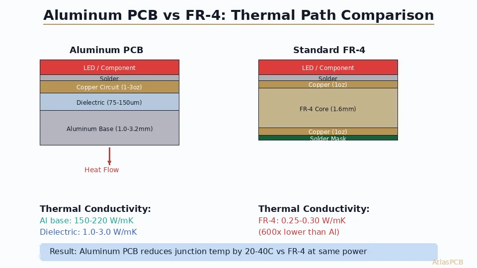
Every electronic component generates heat. For most digital circuits operating at milliwatt levels, standard FR-4 PCBs dissipate heat adequately through copper planes and natural convection. But when power density climbs—high-brightness LED arrays, motor driver ICs handling tens of amps, or power conversion modules operating at hundreds of watts—FR-4’s thermal conductivity of 0.3 W/m·K becomes the bottleneck.
Aluminum PCBs (also called Metal Core PCBs, MCPCBs, or Insulated Metal Substrate boards) solve this by replacing the FR-4 substrate with an aluminum alloy base plate that acts as an integrated heat spreader. The aluminum base provides thermal conductivity of 130-170 W/m·K—over 400× better than FR-4—enabling efficient heat transfer from components to heatsinks or enclosures.
The global aluminum PCB market is growing at approximately 8% CAGR, driven by:
- LED lighting: Street lights, automotive headlamps, commercial fixtures, UV curing systems
- Motor drives: Brushless DC motor controllers, stepper drivers, servo amplifiers
- Power conversion: DC-DC converters, power factor correction, battery chargers
- Automotive electronics: Headlight drivers, ADAS power boards, EV charging modules
- RF power: Base station amplifiers, radar transmitters (where [RF PCB design]/blog/rf-microwave-pcb-design/) meets thermal management)
This guide covers everything you need to design reliable aluminum PCBs, from material selection through manufacturing DFM rules. For related thermal management approaches in standard multilayer boards, see our [PCB thermal via design guide]/blog/pcb-thermal-via-design/) and [PCB thermal management overview]/blog/pcb-thermal-management/).
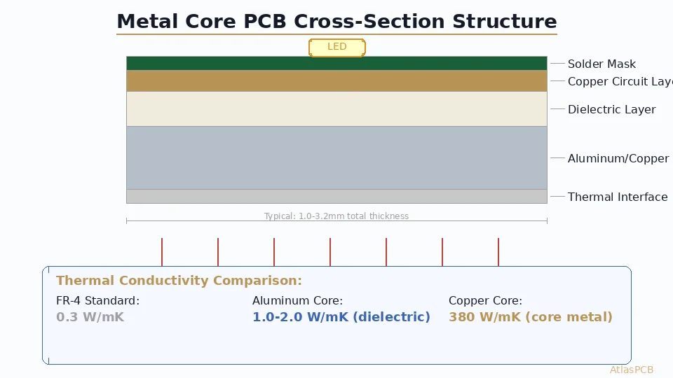
Aluminum PCB Construction: Understanding the Stack
The Three-Layer Structure
A standard aluminum PCB consists of three layers:
1. Copper Circuit Layer (Top) Standard copper foil (1 oz to 10 oz, typically 1-3 oz for most applications) with etched circuit traces. This is where components are soldered. Surface finish options are the same as standard PCBs: HASL, ENIG, OSP—see our [surface finish comparison]/blog/pcb-surface-finish-osp-hasl-enig-immersion-silver-comparison/) for selection guidance.
2. Dielectric Layer (Middle) The critical layer. A thin (50-200 μm typical) thermally-conductive dielectric that provides electrical isolation between the copper circuit and the aluminum base while minimizing thermal resistance. This is where aluminum PCB design lives or dies.
3. Aluminum Base (Bottom) Typically 0.8-3.2 mm thick aluminum alloy plate. Provides mechanical rigidity, lateral heat spreading, and thermal connection to external heatsinks.
Dielectric Layer Deep Dive
The dielectric layer is the performance-defining element of any aluminum PCB. Key parameters:
| Parameter | Standard Grade | Mid Grade | Premium Grade |
|---|---|---|---|
| Thermal conductivity | 1.0-1.5 W/m·K | 2.0-3.0 W/m·K | 3.0-5.0+ W/m·K |
| Typical thickness | 100-150 μm | 75-100 μm | 50-75 μm |
| Breakdown voltage | >3 kV | >3 kV | >3 kV |
| Dielectric constant | ~4.5 | ~4.0 | ~5.5-8.0 |
| Cost multiplier | 1× | 1.5-2× | 3-5× |
Standard grade (1.0-1.5 W/m·K): Suitable for general LED applications under 1W per device, indicator panels, and low-power motor drivers.
Mid grade (2.0-3.0 W/m·K): The sweet spot for most high-power LED arrays, BLDC motor drivers, and power conversion circuits. Recommended as the default starting point for any new aluminum PCB design.
Premium grade (3.0-5.0+ W/m·K): Required for extreme power density applications—automotive headlamps, UV LED curing systems, or power modules exceeding 50W in compact form factors. These use ceramic-filled polymers (aluminum oxide, boron nitride, or aluminum nitride particles) that achieve high thermal conductivity but at significantly higher cost.
Aluminum Alloy Selection
The two common alloys for MCPCB base plates:
5052 Aluminum: General-purpose, good corrosion resistance, moderate thermal conductivity (~138 W/m·K). Used for most LED and standard power applications.
6061-T6 Aluminum: Higher strength, slightly better thermal conductivity (~167 W/m·K), easier to machine for custom heatsink profiles. Preferred for automotive and industrial applications where mechanical mounting loads are significant.
For applications requiring maximum thermal performance, copper-base MCPCBs using C1100 copper (~385 W/m·K) are available but at 3-5× the cost. These are reserved for extreme cases—typically power density exceeding 100 W/cm².
Thermal Design Calculations
Thermal Resistance Model
The thermal path from a component junction to ambient follows a series resistance model:
Tj = Ta + P × (Rjc + Rcs + Rsa)

Where:
Tj  = Junction temperature (°C)
Ta  = Ambient temperature (°C)
P   = Power dissipation (W)
Rjc = Junction-to-case thermal resistance (from datasheet, °C/W)
Rcs = Case-to-sink thermal resistance (solder + dielectric + aluminum, °C/W)
Rsa = Sink-to-ambient thermal resistance (heatsink + convection, °C/W)
For the PCB-specific portion (Rcs), the aluminum PCB contributes:
Rcs_pcb = t_dielectric / (k_dielectric × A) + t_aluminum / (k_aluminum × A_spread)

Where:
t_dielectric = Dielectric thickness (m)
k_dielectric = Dielectric thermal conductivity (W/m·K)
A            = Component thermal pad area (m²)
t_aluminum   = Aluminum thickness (m)
k_aluminum   = Aluminum thermal conductivity (W/m·K)
A_spread     = Effective spreading area in aluminum (m²)
Worked Example: 10W LED Array
Design parameters:
- 4× Cree XP-L2 LEDs, 2.5W each (10W total)
- Rjc per LED: 2.5°C/W
- Ambient: 50°C (enclosed fixture)
- Target: Tj < 120°C (Tj_max = 150°C, 30°C margin)
Available thermal budget per LED:
- ΔT = 120 - 50 = 70°C
- Per LED: Rjc contribution = 2.5W × 2.5°C/W = 6.25°C
- Remaining for PCB + heatsink: 70 - 6.25 = 63.75°C per LED
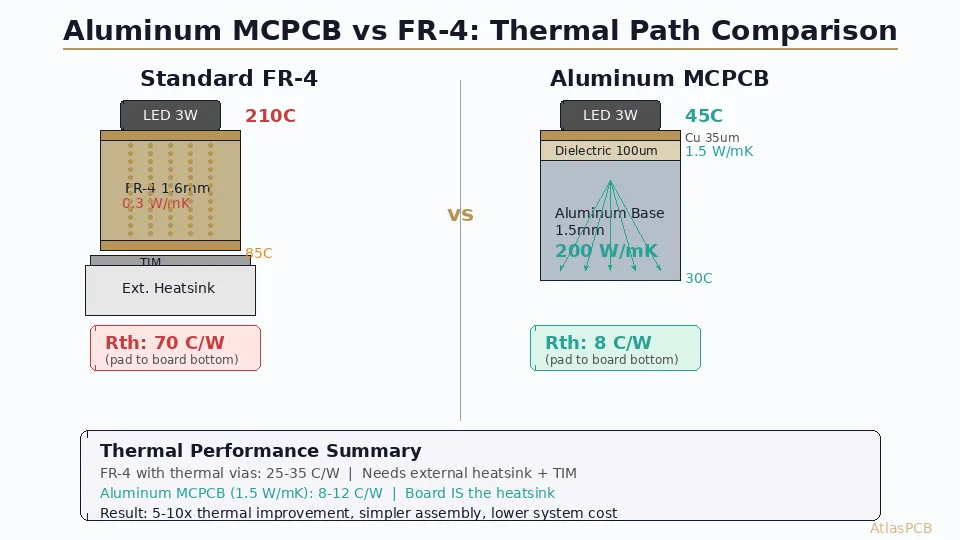
With standard FR-4 (0.3 W/m·K, 1.6mm thick):
- Rcs_FR4 ≈ 0.0016 / (0.3 × 9×10⁻⁶) = 593°C/W per LED pad
- Board temperature rise: 2.5W × 593°C/W = 1483°C — Impossible!
With aluminum PCB (2.0 W/m·K dielectric, 75μm thick, 1.5mm aluminum):
- Rcs_dielectric ≈ 0.000075 / (2.0 × 9×10⁻⁶) = 4.2°C/W
- Rcs_aluminum ≈ negligible (aluminum spreading resistance ~0.1°C/W)
- Board temperature rise: 2.5W × 4.3°C/W = 10.75°C — Easily manageable
This leaves 63.75 - 10.75 = 53°C budget for the heatsink-to-ambient path, which is comfortable for a modest finned heatsink with natural convection.
Need an Aluminum PCB for Your LED or Power Design?
AtlasPCB manufactures aluminum MCPCBs with dielectric thermal conductivity from 1.0 to 5.0 W/m·K. Our engineering team reviews every thermal design before production.
Get a Thermal Design Review →LED Array Design on Aluminum PCBs
Thermal Pad Layout
For high-power LEDs, the thermal pad underneath the package is the primary heat extraction path. Design rules:
- Thermal pad size: Match the LED package datasheet exactly. Oversized pads waste board area; undersized pads create solder voids that act as thermal barriers
- Solder paste coverage: Use 80-90% coverage on thermal pads (not 100%—outgassing needs escape paths). Stencil aperture should be segmented into a grid pattern
- Via prohibition: Unlike standard PCBs where [thermal vias]/blog/pcb-thermal-via-design/) help transfer heat through the board, aluminum PCBs should NOT have vias through the dielectric—this compromises electrical isolation. The entire dielectric layer IS the thermal path
- Copper pour: Maximize copper coverage around LED pads. The copper layer helps with lateral heat spreading before heat enters the dielectric. Use thermal relief connections only for hand-soldering applications; for reflow, direct connections provide better thermal performance
LED Spacing and Thermal Interaction
When multiple LEDs share an aluminum PCB, their thermal zones interact. Each LED heats the aluminum beneath it, and these heat zones overlap if LEDs are too close:
- Minimum spacing: Allow at least 2× the aluminum thickness between LED thermal pads for adequate lateral spreading
- Edge effects: LEDs near board edges run hotter because heat can only spread in limited directions. Add 30% thermal margin for edge-mounted LEDs
- Thermal simulation: For arrays of 8+ LEDs, CFD simulation is recommended to verify hotspot temperatures. Simple 1D calculations underestimate peak temperatures in dense arrays
Color Temperature and Thermal Design
LED color temperature shifts with junction temperature—approximately -2 to -3 nm per 10°C for white LEDs (shift toward blue/cooler). For lighting applications where color consistency matters (architectural, retail, medical), this means thermal design directly impacts product quality, not just reliability.
Design target for color-critical applications: ΔTj < 10°C across all LEDs in the array, which requires uniform thermal path design and balanced power distribution.
Motor Driver Design on Aluminum PCBs
Why Motor Drivers Need Metal Core Boards
BLDC motor drivers, H-bridge ICs, and MOSFET driver circuits routinely dissipate 5-50W of heat in compact packages. The combination of high continuous current (10-50A), switching losses, and small package sizes creates power densities that overwhelm standard FR-4.
Common motor driver ICs designed for aluminum PCBs:
| IC | Package | Max Power | Recommended Dielectric |
|---|---|---|---|
| DRV8353 (TI) | HTQFP-48 | 15W | ≥2.0 W/m·K |
| L6235 (ST) | PowerSSO-36 | 10W | ≥1.5 W/m·K |
| TMC2160 (Trinamic) | QFN-48 | 8W | ≥1.5 W/m·K |
| Custom MOSFET stage | D2PAK/TO-263 | 50W+ | ≥3.0 W/m·K |
Layout Rules for Power Stages
- MOSFET placement: Position high-side and low-side MOSFETs to spread heat load across the aluminum base. Avoid clustering all power devices in one corner
- Current handling: For high-current traces (>10A), use 3 oz or heavier copper. Calculate trace width using IPC-2152 guidelines—see our [trace width calculator guide]/blog/pcb-trace-width-current-capacity/)
- Gate drive routing: Keep gate drive traces short and low-inductance. Use wide, short traces rather than vias (remember: no through-board vias on standard aluminum PCBs)
- Sense resistors: Place current sense resistors on the same thermal zone as the MOSFETs they monitor—thermal gradients between power devices and sense elements cause measurement error
- Bulk capacitors: Electrolytic capacitors near power MOSFETs will run hot. Consider placing them on a standard FR-4 daughter board connected via headers, or use ceramic capacitors that tolerate higher temperatures
Manufacturing DFM Rules for Aluminum PCBs
Drilling and Routing
- No plated through holes: Standard aluminum PCBs cannot have plated through holes because the aluminum base is conductive. All connections must be routed on the single copper layer
- Scoring: V-score panelization works well with aluminum (better than tab routing, which leaves burrs in the soft aluminum)
- CNC routing: Use carbide tooling designed for aluminum. Feed rates and spindle speeds differ significantly from FR-4. Router bit diameter minimum: 1.6mm for aluminum
- Hole drilling: Non-plated mounting holes through the full stack are possible but require specialized tooling. Specify aluminum-compatible drill in your fab notes
Solder Mask
- White solder mask: Standard for LED applications (reflectivity improves light output by 5-15%)
- Adhesion: Solder mask adhesion to copper over aluminum substrates requires proper plasma treatment of the dielectric surface. Specify IPC Class 2 or 3 adhesion testing in your procurement spec
- Thermal cycling: The CTE mismatch between aluminum (23 ppm/°C) and solder mask (~60 ppm/°C) is larger than with FR-4, making solder mask cracking a risk in high-temperature-cycling applications. Consider conformal coating for harsh environments—see our [conformal coating guide]/blog/conformal-coating-pcb/)
Assembly Considerations
- Reflow soldering: Aluminum’s high thermal mass means the board absorbs significant heat during reflow. The [reflow profile]/blog/reflow-soldering-profile-optimization-lead-free-pcb-assembly/) must account for this—preheat zone may need to be extended to ensure the aluminum base reaches adequate temperature for proper solder wetting on the top side
- Board support: The aluminum base provides excellent flatness during reflow—better than FR-4. However, thin aluminum boards (0.8mm) can warp under thermal stress. Use 1.0mm minimum for boards larger than 100×100mm
- Depaneling: Score lines must be deep enough for clean separation but not so deep that they compromise heat spreading. Target 30-40% of total board thickness for V-score depth
Design for Test (DFT) Considerations
Since standard aluminum PCBs are single-layer, test access is inherently limited:
- Test points: Add probe-accessible test pads for all critical nets. Without inner layers for routing, test point placement is constrained by the single-layer routing
- Flying probe: Flying probe test is the standard electrical test method for aluminum PCBs. In-circuit test fixtures are also possible but require careful probe force management to avoid denting the aluminum base
- Thermal testing: For production verification, specify infrared thermal imaging or thermocouple testing of representative samples at rated power to validate thermal performance
Conclusion: Design Checklist
Before sending your aluminum PCB design for fabrication:
- Dielectric thermal conductivity specified (≥2.0 W/m·K for most power applications)
- Aluminum thickness adequate for heat spreading (≥1.0mm for LED, ≥1.5mm for motor drivers)
- Thermal calculations show Tj < Tj_max - 20°C at worst-case ambient
- No through-hole vias specified (single-layer design confirmed)
- Copper weight adequate for current handling (IPC-2152 compliance)
- Solder mask type specified (white for LED, green for general power)
- Reflow profile notes included (extended preheat for aluminum thermal mass)
- V-score panelization specified (preferred over tab routing)
- Mounting hole locations compatible with heatsink/enclosure interface
Ready to manufacture your aluminum PCB? AtlasPCB’s aluminum PCB production line handles boards from 0.8mm to 3.2mm aluminum thickness with dielectric conductivity up to 5.0 W/m·K. We provide DFM review and thermal simulation as part of our engineering review process. Upload your design for a quote →
Further Reading
- [PCB Design for GaN and SiC Power Devices: Thermal Management, Layout Rules, and Material Selection]/blog/pcb-design-gan-sic-power-devices-thermal-layout/)
- [AI Hardware PCB Thermal Management: Advanced Multilayer Stackup Design for 1000W+ Processing Units]/blog/ai-hardware-pcb-thermal-management-multilayer-design/)
- [PCB Panelization and Array Design: V-Score vs Tab Routing, DFM Rules, and Cost Optimization]/blog/pcb-panelization-v-score-tab-routing-dfm-cost-optimization/)
- [PCB Manufacturer with Engineering Review: Why Human DFM Audit Matters]/blog/pcb-manufacturer-engineering-review/)
- [阻焊坝设计 — 规则、公差与DFM最佳实践]/blog/pcb-solder-mask-dam-design-rules-dfm/)
- Rigid PCB Manufacturing
About AtlasPCB — We specialize in complex PCB manufacturing for HDI, RF, and high-reliability applications. Explore our aluminum PCB manufacturing, or get an free engineering DFM review . Every order includes free engineering review. Get your quote.
Reviewed by AtlasPCB Engineering Team — IPC-certified manufacturing specialists with 15+ years of production experience in HDI, RF, and high-reliability PCB fabrication. Content based on factory floor data and real customer design reviews.
- aluminum PCB
- MCPCB
- metal core PCB
- thermal management
- LED PCB
- motor driver
- thermal conductivity
- dielectric layer
- DFM
- IMS