· AtlasPCB Engineering · Engineering · 8 min read
JLCPCB vs Custom PCB Manufacturer: When Budget Prototyping Falls Short
Comparing JLCPCB's automated low-cost model against dedicated custom PCB manufacturers. Understand where each excels — from $2 prototypes to controlled-impedance RF boards — and how to choose based on your project's actual requirements.
The 30-Second Decision
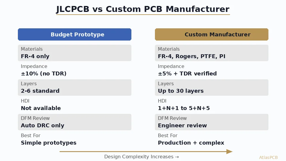
| Factor | JLCPCB | Custom PCB Manufacturer |
|---|---|---|
| Best for | Standard 2-4L FR-4 prototypes | Complex, high-reliability, specialty materials |
| Pricing (5pc prototype) | $2-30 | $80-500 |
| Impedance tolerance | ±10% (add-on) | ±5% with TDR verification |
| Materials | FR-4, aluminum | FR-4, Rogers, PTFE, polyimide, metal core |
| Max layers (standard) | 6 (8 with extended) | 30+ |
| Engineering support | Automated DRC only | Dedicated DFM engineer review |
| Lead time | 1-5 days | 5-18 days (1-day rush available) |
| Minimum trace/space | 5/5mil | 3/3mil (75μm) |
If your design is a standard digital board with nothing exotic, JLCPCB delivers unbeatable value. The moment you need RF performance, tight impedance, specialty materials, or production-grade consistency, a custom manufacturer is not optional — it is the only path to a working product.
Where JLCPCB Excels
The JLCPCB model works because of extreme automation and standardization. Their factories process tens of thousands of orders daily using fixed process parameters optimized for the most common PCB configurations. This high-volume, low-margin approach delivers legitimate value for a specific category of work.
Standard 2-layer and 4-layer FR-4 boards with 6/6mil trace/space, 0.3mm minimum drill, and HASL finish represent roughly 70% of all prototype orders globally. For these configurations, JLCPCB’s automated panelization, fixed stackup library, and batch processing yield boards that are perfectly adequate for digital logic validation, power supply testing, and IoT device development. The quality is consistent within their standard parameters because the process is so tightly controlled through repetition.
The $2 price point for 5 prototype boards fundamentally changed how hardware engineers iterate. Where a decade ago you might carefully verify a design before committing $300 to a prototype run, today you can spin three variations simultaneously and test them all. This rapid iteration capability has genuine engineering value — as long as you understand what you are actually receiving.
DESIGN COMPLEXITY CHECK
Not Sure If Your Design Needs Custom Fabrication?
Upload your Gerber files — our engineers review complexity, material requirements, and impedance needs within 24 hours. No commitment required.
Upload Gerber Files ›Where JLCPCB Falls Short
The limitations become apparent the moment your design departs from the standard envelope. In our facility, we regularly receive orders from engineers who started with JLCPCB prototypes, passed initial functional testing, then discovered performance problems when moving to production or higher-frequency operation.
Impedance Control: The 10% Problem
JLCPCB’s impedance control service specifies ±10% tolerance with no individual coupon verification. For a 50-ohm trace, this means your actual impedance could land anywhere from 45 to 55 ohms. On a USB 2.0 line operating at 480 MHz, this might be acceptable. On a PCIe Gen4 link at 16 GT/s or a DDR5 interface, that 10% variation introduces enough reflection to corrupt signals at the receiver.
Our process engineering team runs TDR verification on every impedance-controlled panel, providing actual measured data — not just a promise that the process was nominally set up correctly. The difference between ±5% guaranteed (with test coupon data) and ±10% nominal (with no verification) is the difference between a board that works at speed and one that requires months of signal integrity debugging.
Material Limitations
When your application demands low-loss dielectrics — whether Rogers RO4350B for a 5 GHz RF front-end, high-Tg FR-4 for automotive under-hood electronics, or polyimide for a flexible interconnect — the automated ordering system cannot accommodate these requirements. Each specialty material requires specific processing parameters: drill speeds, plating chemistry adjustments, lamination temperature profiles, and press cycle modifications that only work when an experienced process engineer configures the line specifically for your stackup.
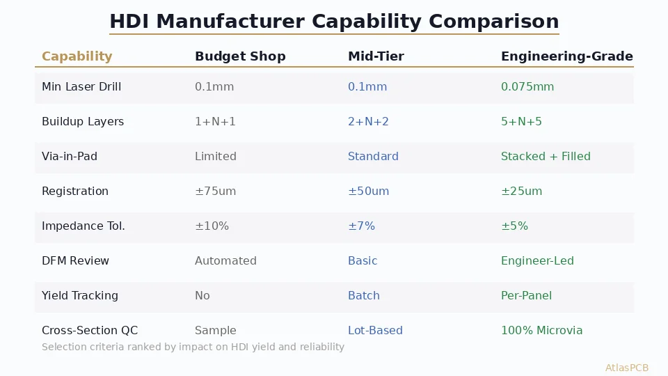
HDI and Advanced Via Structures
Laser-drilled microvias, sequential lamination, stacked vias, via-in-pad with planarization — these structures require dedicated engineering attention at every step. In our experience producing 5+N+5 HDI boards, the registration accuracy between sequential lamination cycles must be maintained within ±25μm. This level of precision demands operator expertise and in-process inspection that automated high-volume flows cannot provide at $2 per board.
RF AND HIGH-SPEED SPECIALIST
Rogers, PTFE, Hybrid Stackups — Fabricated Right
We process RO4350B, RO4003C, PTFE, and hybrid Rogers/FR-4 stackups daily. TDR-verified impedance, cross-section analysis available.
The Real Cost Comparison: Beyond Board Price
Engineers often compare the $5 JLCPCB board against a $200 custom manufacturer quote and conclude the choice is obvious. But the total cost of ownership tells a different story when design complexity increases.
Prototype Phase Cost Analysis
Consider a 6-layer controlled-impedance board for a DDR4 memory interface:
| Cost Element | JLCPCB Route | Custom Manufacturer Route |
|---|---|---|
| Board fabrication (5pc) | $35 | $180 |
| First article impedance failure rate | ~40% | <5% |
| Respin NRE (layout engineer time) | $2,000-5,000 | $0 (caught in DFM) |
| Schedule slip (2-3 week respin) | $3,000-10,000 opportunity cost | None |
| Total probable cost | $5,035-15,035 | $180 |
We see this pattern repeatedly: an engineer orders from JLCPCB, receives boards that pass basic continuity testing, then discovers signal integrity issues during high-speed validation. The “savings” on board cost evaporate against one respin cycle that a proper DFM review would have prevented.
Production Volume Economics
At production volumes (1,000+ pieces), the per-unit economics shift further. JLCPCB’s pricing advantage diminishes because their model is optimized for small-batch variety, not volume efficiency. A custom manufacturer running your specific design on dedicated panels achieves better yield rates, tighter process windows, and lower per-unit costs because the setup is amortized across a larger run.
For a 4-layer board at 1,000 pieces, a custom manufacturer typically quotes $3-6 per unit (depending on complexity), compared to JLCPCB’s $4-8 range for the same quantity. The crossover point where custom manufacturing becomes cheaper is often lower than engineers expect — typically around 200-500 pieces for boards with any controlled-impedance requirements.
PRODUCTION PRICING
Volume Pricing That Beats Prototype Services
Our production pricing for 500+ pieces often matches or beats JLCPCB per-unit cost — with guaranteed impedance, IPC-600 Class 2/3 inspection, and full traceability.
Compare Pricing ›Decision Framework: When to Use Each
Use JLCPCB When:
Your design meets ALL of these criteria: standard FR-4 material (Tg 135-150), 2-4 layers with standard stackup, trace/space at or above 5/5mil, no controlled impedance requirements (or ±10% is acceptable), through-hole vias only (0.3mm+), HASL or ENIG finish with standard specs, prototype quantities (1-50 pieces), and no regulatory compliance documentation needed.
Use a Custom Manufacturer When:
Your design includes ANY of these requirements: controlled impedance with ±5% tolerance and TDR verification, Rogers, PTFE, polyimide, or metal-core materials, HDI with microvias or sequential lamination, layer counts above 6, trace/space below 5/5mil, rigid-flex construction, production quantities above 200 pieces, aerospace/medical/automotive compliance (IPC Class 3, AS9100, ISO 13485), or engineering DFM review before fabrication.
The Hybrid Approach
Many successful hardware teams use both: JLCPCB for early-stage digital prototypes and custom manufacturers for final validation and production. The key is knowing when to transition. Our recommendation: use budget services for anything where electrical performance is not critical to your test goals, and switch to a custom manufacturer the moment you need to validate RF performance, signal integrity at speed, or production-representative reliability.
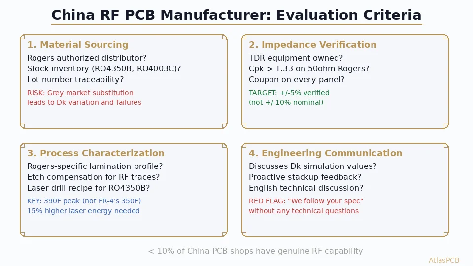
Choosing a Custom PCB Manufacturer in China
If you have decided that your project needs custom fabrication, selecting the right manufacturer requires evaluating specific capabilities rather than simply choosing the cheapest quote. Key evaluation criteria include: impedance control tolerance and verification method (ask for sample TDR reports), material certifications and procurement channels (legitimate Rogers distributors vs. grey market), maximum layer count and HDI buildup they have actually produced (ask for reference photos), quality certifications relevant to your industry (IPC, AS9100, ISO 13485, IATF 16949), and engineering communication quality (can they discuss your stackup intelligently in English?).
The China PCB manufacturing landscape ranges from fully automated high-volume consumer electronics factories to specialized shops handling complex military and aerospace boards. The $2 prototype services and the ±5% impedance-controlled RF houses serve fundamentally different markets — understanding which market your design belongs in saves time, money, and frustration.
ATLASPCB
Ready to Move Beyond Budget Prototyping?
Upload your design files for a detailed quote with DFM review. We handle Rogers, HDI, rigid-flex, and impedance-controlled boards — from prototype through production.
Get Detailed Quote ›Reviewed by AtlasPCB Engineering Team — 15+ years in advanced PCB fabrication for RF, HDI, and rigid-flex applications.
Related Reading:
- Custom PCB Manufacturing Services
- PCB Manufacturer China: Engineering-Grade Fabrication
- FR-4 vs Rogers PCB: Complete Material Selection Guide
- Impedance Controlled PCB Manufacturer: ±5% Guaranteed
- HDI PCB Stackup Design: Sequential Lamination and Any-Layer HDI
- Signal Integrity in PCB Design: Impedance Control and Crosstalk
About AtlasPCB — We specialize in complex PCB manufacturing for HDI, RF, and high-reliability applications. Explore our full PCB manufacturing capabilities, or get an instant online quote . Every order includes free engineering review. Get your quote.
Reviewed by AtlasPCB Engineering Team — IPC-certified manufacturing specialists with 15+ years of production experience in HDI, RF, and high-reliability PCB fabrication. Content based on factory floor data and real customer design reviews.
- JLCPCB
- custom PCB manufacturer
- PCB prototyping
- PCB fabrication
- China PCB manufacturer