· AtlasPCB Engineering · Engineering · 10 min read
HDI PCB Manufacturer Selection: Budget Board House vs Engineering-Grade Fabricator
How to evaluate HDI PCB manufacturers beyond price per panel. Compares budget shops offering basic 1+N+1 buildup against engineering-grade fabricators with stacked microvias, via-in-pad, and per-panel yield tracking — with decision criteria for prototype vs production.
Quick Answer: Which HDI Manufacturer Tier Do You Need?
| Your Design Requirement | Budget Shop | Engineering-Grade |
|---|---|---|
| 1+N+1 buildup, 0.1mm vias | Yes | Overkill |
| 2+N+2 with stacked microvias | Risky | Yes |
| 3+N+3 or higher | No | Yes |
| Via-in-pad (BGA < 0.8mm pitch) | Low yield | Yes |
| Impedance ±5% on HDI layers | No | Yes |
| Line/space 75/75um or finer | Marginal | Yes |
| Production > 500 pcs HDI | Cost risk | Better TCO |
If your design stays within 1+N+1 buildup with standard laser drill sizes and you are only building 5-10 prototypes to validate functionality, a budget shop is perfectly adequate. The moment you push into stacked vias, tight registration requirements, or production volumes where yield matters, the economics shift dramatically.
Understanding the HDI Manufacturer Landscape
The HDI PCB manufacturing market in 2026 has stratified into distinct capability tiers, and the naming conventions manufacturers use can be misleading. A shop advertising “HDI capability” might mean they own a single UV laser drill and can produce basic 1+N+1 boards — or it might mean they run sequential lamination with ±25um registration across five buildup cycles. The gap between these two extremes is enormous, and choosing the wrong tier for your design complexity is one of the most common — and expensive — mistakes hardware engineers make.
In our facility, we regularly receive “rescue jobs” from engineers who prototyped at a budget shop, got boards that looked correct under visual inspection, but failed during electrical test or assembly. The most common failure mode is microvia reliability: budget shops achieve acceptable first-pass yield on single-buildup HDI, but their process control degrades rapidly on stacked structures where each sequential lamination cycle compounds registration errors and via fill defects.
The real cost of an HDI board is not the purchase price — it is the total cost including respins, yield fallout, and assembly failures caused by fabrication defects that were never caught because the shop does not inspect at the granularity your design demands.
HDI FABRICATION EXPERTISE
Up to 5+N+5 Buildup with Stacked Microvias
Per-panel cross-section QC, ±25um registration, conductive via fill with X-ray verification.
Upload Your HDI Design ›The Five Critical Differentiators
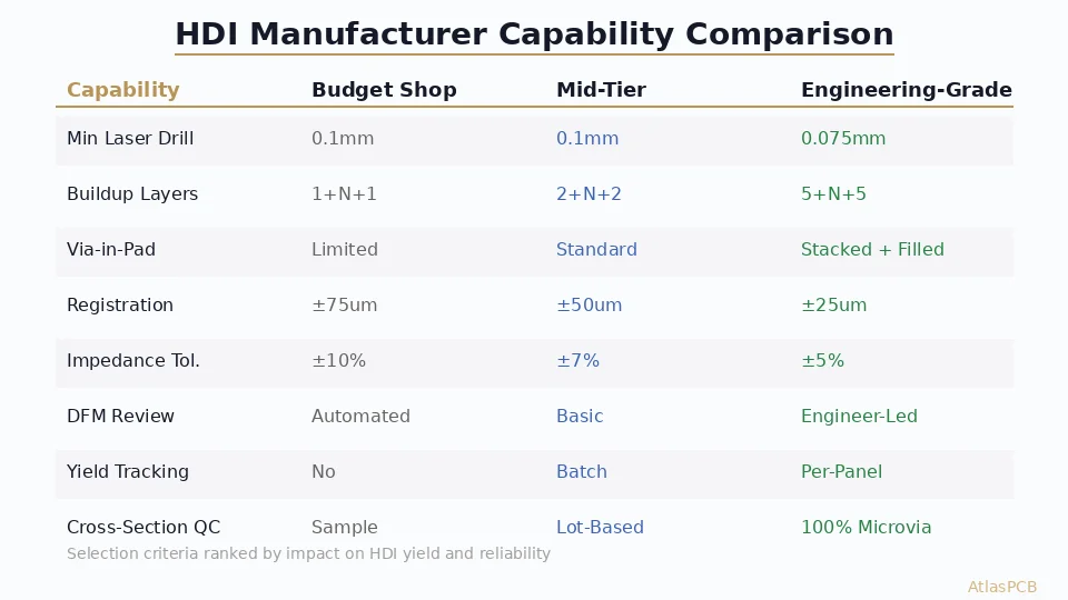
1. Laser Drill Capability and Via Quality
The laser drill is the single most expensive piece of equipment in an HDI line, and its capability defines the floor of what a manufacturer can produce. Budget shops typically operate older CO2 laser systems that reliably drill down to 0.1mm (100um) diameter with acceptable taper angles. Engineering-grade fabricators run UV or UV-CO2 hybrid systems capable of 0.075mm (75um) vias with superior sidewall quality and less thermal damage to surrounding dielectric.
The diameter itself is only part of the story. What matters for your design is the aspect ratio of the microvia (depth divided by diameter) and the quality of subsequent copper plating into that via. A 0.1mm via through a 0.065mm dielectric (standard prepreg thickness) has an aspect ratio of 0.65:1 — easy to plate reliably. Push that to 0.075mm through the same dielectric and you hit 0.87:1, which requires tighter plating bath chemistry control and throws distribution uniformity to maintain void-free fill.
We track microvia void rate across every production lot. On standard 0.1mm vias through single dielectric layers, our void rate runs below 2%. On 0.075mm stacked vias with conductive fill, we hold below 5% — a number that took eighteen months of process optimization to achieve consistently.
2. Sequential Lamination Registration
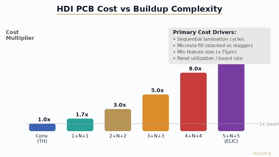
Every HDI buildup layer requires a sequential lamination cycle — the board is built up one layer at a time rather than pressed in a single stack. Each cycle introduces alignment error between the newly drilled via and the target pad below. For 1+N+1, this is one registration step. For 3+N+3, it is three per side — six total opportunities for misalignment to compound.
Budget manufacturers typically hold ±75um layer-to-layer registration, which is adequate for 1+N+1 designs with generous annular ring targets (150um pad on 100um via = 25um annular ring each side, with registration eating into that budget). Engineering-grade shops achieve ±25-35um through X-ray alignment systems, direct imaging, and climate-controlled lamination rooms.
The practical implication: on a 2+N+2 design with 0.1mm vias landing on 0.25mm pads, budget registration of ±75um consumes your entire annular ring tolerance on the second buildup layer. At ±25um, you maintain 50um of margin — the difference between 90% yield and 60% yield.
3. Impedance Control on HDI Layers
Controlling impedance on HDI buildup layers presents unique challenges compared to conventional through-hole boards. The thin dielectrics (50-75um typical) used in HDI construction amplify the sensitivity of impedance to trace width variations. A ±5um etch variation on a 75um trace over 65um dielectric swings impedance by approximately ±4 ohms on a 50-ohm target — which is ±8%.
Budget shops that offer ±10% impedance tolerance on their standard boards often cannot maintain even that on HDI buildup layers without special attention. Engineering-grade manufacturers address this through modified etch parameters for thin-dielectric layers, pre-etch impedance prediction with dielectric thickness verification via cross-section, and panel-level TDR measurement on every impedance-critical lot.
If your HDI design carries high-speed signals (PCIe Gen4+, DDR5, USB4) on buildup layers, impedance control is not optional — it is the primary fabrication challenge. Ask your manufacturer specifically about their impedance capability on HDI layers, not just their general ±5% specification that may apply only to core layers.
IMPEDANCE VERIFICATION
TDR Testing on Every HDI Production Panel
±5% impedance on buildup layers with per-panel coupon measurement and full test reports.
View Our Capabilities ›4. Via-in-Pad Execution Quality
Via-in-pad (VIPPO — Via In Pad Plated Over) is the most commonly mishandled HDI process across the industry. Every shop offers it. Very few execute it consistently at production volumes. The failure mode is subtle: partially filled vias that pass visual inspection but leave internal voids. These voids become gas traps during reflow soldering, causing solder blowout or insufficient wetting under BGA balls.
Engineering-grade manufacturers use conductive copper fill (electroplated) followed by surface planarization, achieving fill rates above 95% with void dimensions below 25um. They verify this with X-ray inspection on a statistical or 100% basis depending on customer requirements. Budget shops typically use non-conductive epoxy fill, which is cheaper but produces larger voids (50-100um typical) and can crack under thermal cycling.
For BGA components with pitch 0.65mm or finer, the via-in-pad fill quality directly determines your assembly yield. We have measured a consistent correlation in our production data: boards with >5% via fill void rate show 3-5% higher BGA assembly defect rate compared to boards with <2% void rate. On a 1500-ball BGA, that translates to dozens of potential open or intermittent connections.
5. Quality Control Granularity
Perhaps the most significant — and least visible — difference between manufacturer tiers is inspection granularity. Budget shops operate on lot-based sampling: they cross-section one board per production lot (typically 25-50 panels) and extrapolate quality to the entire batch. If that one sample passes, everything ships. If the process drifted during the run, the other 49 panels may contain defects.
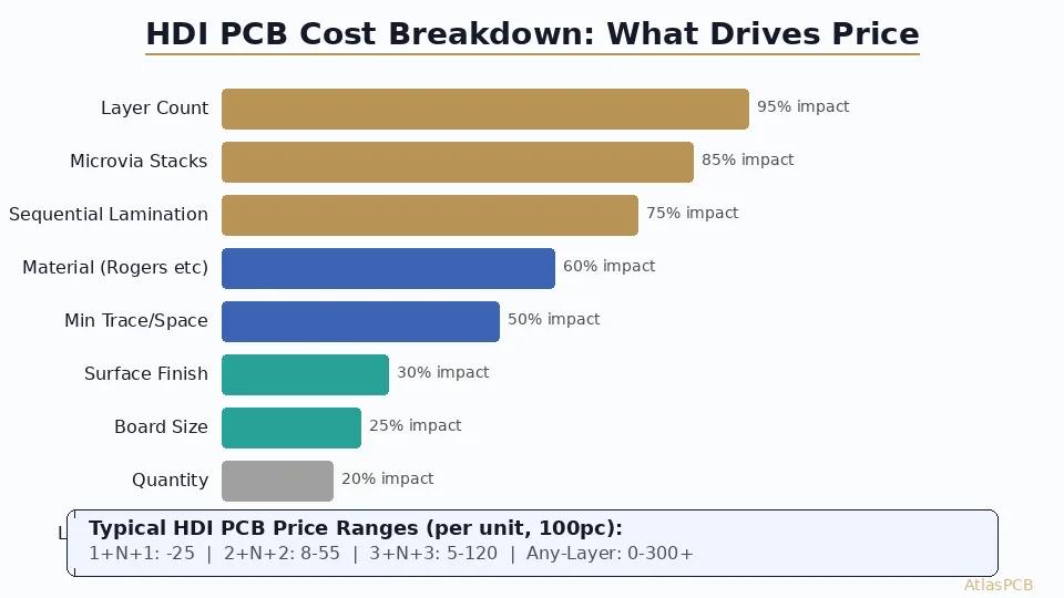
Engineering-grade manufacturers perform per-panel or per-batch inspection with multiple cross-section locations, automated optical inspection of every via on every panel, and impedance testing of dedicated coupons that accompany each panel through the process. The cost difference is substantial — roughly 15-25% of the total board price goes to inspection and documentation for high-reliability HDI — but it provides statistical confidence that every board in your shipment meets specification.
For prototype work where you will validate boards through your own testing anyway, lot-based QC from a budget shop may be perfectly acceptable. For production boards going directly into assembled products, especially those with BGAs or fine-pitch components where rework is impractical, the per-panel QC of an engineering-grade shop prevents costly field failures.
ENGINEERING SUPPORT
Pre-Production DFM Review by Process Engineers
Our HDI team reviews your stackup, via structures, and impedance requirements before production starts — catching issues that automated tools miss.
Total Cost of Ownership: When Premium Makes Economic Sense
The following comparison illustrates why per-board price is misleading for HDI:
| Scenario | Budget Shop | Engineering-Grade |
|---|---|---|
| Board price (6L 2+N+2, 10pcs) | $120/board | $320/board |
| First-pass yield | 65% | 92% |
| Boards received (usable) | 6-7 of 10 | 9-10 of 10 |
| Effective cost per good board | $171-$185 | $320-$356 |
| Assembly scrap (via fill defects) | 8-12% | 1-2% |
| Respin probability | 25-35% | 5-10% |
| Respin cost (time + new build) | $3000-5000 | — |
At prototype volumes (5-10 pieces), the budget shop wins on cash outlay even accounting for yield loss — provided you can absorb the schedule risk of a potential respin. At production volumes (500+ pieces), the yield difference alone makes the engineering-grade shop cheaper per delivered good board. Factor in assembly yield improvements and the elimination of field failures, and the economic case becomes overwhelming for any design that pushes HDI capabilities.
The engineers who consistently choose the right manufacturer tier are those who understand their design’s actual demands versus what the manufacturer can reliably produce — not just what they advertise on their capability sheet.
Decision Framework: Choosing Your HDI Partner
Choose a budget shop when:
- Design is 1+N+1 with standard 0.1mm vias
- Prototype only (not production intent)
- No impedance control on HDI layers
- BGA pitch 1.0mm or larger
- Timeline allows for potential respin
Choose an engineering-grade fabricator when:
- Design is 2+N+2 or higher buildup
- Stacked or staggered microvias required
- Via-in-pad under fine-pitch BGA (< 0.8mm)
- Impedance control ±5% on buildup layers
- Production volumes where yield drives cost
- Reliability requirements (automotive, medical, aerospace)
- Schedule cannot accommodate respin risk
ATLASPCB
Ready to Validate Your HDI Design?
Upload your Gerber files for a free manufacturability assessment. Our HDI process engineers review stackup, via structures, and impedance feasibility before quoting.
Upload Gerber Files ›Reviewed by AtlasPCB Engineering Team — 15+ years in advanced PCB fabrication for RF, HDI, and rigid-flex applications.
Related Reading:
About AtlasPCB — We specialize in complex PCB manufacturing for HDI, RF, and high-reliability applications. Explore our HDI PCB manufacturing capabilities . Every order includes free engineering review. Get your quote.
Reviewed by AtlasPCB Engineering Team — IPC-certified manufacturing specialists with 15+ years of production experience in HDI, RF, and high-reliability PCB fabrication. Content based on factory floor data and real customer design reviews.
- HDI PCB manufacturer
- microvia PCB
- HDI fabrication
- PCB supplier selection
- via-in-pad