· AtlasPCB Engineering · Engineering · 13 min read
PCB Edge Plating Guide: Castellation, EMI Shielding, and Wrap-Around Plating Design
Complete engineering guide to PCB edge plating techniques including castellation, wrap-around plating, and edge metallization for EMI shielding, RF grounding, and module interconnection. Covers IPC-6012 Class 3 requirements, manufacturing processes, and design rules.

PCB Edge Plating Guide: Castellation, EMI Shielding, and Wrap-Around Plating Design
Edge plating is one of those PCB manufacturing techniques that sits at the intersection of electrical engineering, mechanical design, and electromagnetic compatibility. While most PCB features are confined to the XY plane of the board, edge plating extends metallization to the Z-axis — the board edges themselves — creating continuous conductive paths from top to bottom layer along the routed perimeter.
This guide covers the engineering fundamentals, IPC requirements, manufacturing processes, and design rules for three primary edge plating applications: EMI shielding enclosures, castellated module interconnections, and RF cavity grounding. Whether you’re designing a Bluetooth module that needs castellation for soldering to a carrier board, or an RF subsystem requiring a continuous ground cage, the principles here will help you get the design right the first time.
What is PCB Edge Plating?
PCB edge plating (also called edge metallization, plated edges, or wrap-around plating) is the process of depositing copper — and optionally surface finish metals like nickel/gold or tin — on the routed edges of a printed circuit board. This creates a conductive surface on the board edge that electrically connects copper features on the top layer, bottom layer, and any internal layers that extend to the board perimeter.
The three primary applications are:
- EMI Shielding — Creating a continuous Faraday cage around sensitive circuitry by connecting top and bottom ground planes through plated board edges
- Castellation — Half-plated holes along the board edge for module-to-PCB soldering (common in wireless modules, sensor modules, and power modules)
- RF Grounding — Providing low-inductance ground connections for RF cavities and waveguide structures in microwave circuit boards
How Edge Plating Differs from Standard Via Plating
Standard [via plating]/blog/pcb-via-types-guide/) deposits copper inside drilled holes within the board interior. Edge plating deposits copper on the board’s routed edge surfaces. The key differences:
| Parameter | Standard Via | Edge Plating |
|---|---|---|
| Location | Interior of board | Board edge/perimeter |
| Process | Drill → plate → route | Drill → plate → route through plated area |
| Copper thickness | ≥ 20μm (IPC-6012) | ≥ 25μm (IPC-6012) |
| Surface finish | Via fill or mask | Same as board surface finish |
| Design constraint | Annular ring rules | Edge keepout zone rules |
IPC-6012 Requirements for Edge Plating
IPC-6012 (Qualification and Performance Specification for Rigid Printed Boards) establishes the baseline requirements for edge plating quality and reliability.
Copper Thickness Requirements
- Class 1 (General Electronic Products): Minimum 20μm average copper thickness on plated edges
- Class 2 (Dedicated Service Electronic Products): Minimum 25μm average copper thickness
- Class 3 (High Reliability Electronic Products): Minimum 25μm with no single measurement below 20μm
For EMI shielding applications requiring continuous coverage, the practical minimum is 35μm to account for thinning at corners and transitions. Many [high-reliability manufacturing processes]/blog/pcb-manufacturing-process/) target 50μm for critical RF applications.
Adhesion Requirements
Per IPC-6012 §3.6, the plated copper on board edges must demonstrate adequate adhesion:
- No delamination after thermal stress testing (6× solder float at 288°C for 10 seconds)
- No cracking after thermal cycling (-65°C to +125°C, 100 cycles for Class 3)
- Peel strength ≥ 0.7 N/mm for Class 3 applications
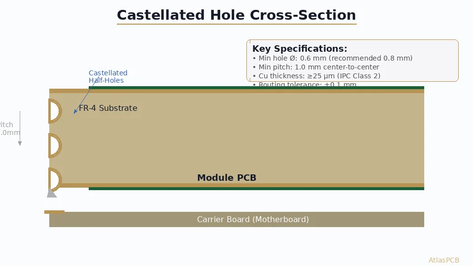
Castellation-Specific Requirements
IPC-6012 §3.6.2.11 covers plated castellations (half-holes):
- Minimum plating thickness in the castellation: 25μm (same as edge plating)
- Castellation geometry: The half-hole must be ≥ 50% of the original drilled hole
- Plating must be continuous from the top pad through the castellation to the bottom pad
- No cracks, voids, or delamination visible at 10× magnification
Manufacturing Process: How Edge Plating is Made
Method 1: Score-and-Break (for Castellation)
This is the most common method for castellated edges on module PCBs:
Panel design: PCBs are arrayed in the panel with shared edges. Plated through-holes (PTH) are placed at the intended castellation locations, straddling the board outline.
Standard PTH plating: The holes are drilled, desmeared, and plated using the normal [multilayer PCB manufacturing process]/blog/multilayer-pcb-manufacturing-process-explained/). Copper thickness in the hole barrel meets the same 25μm minimum as standard vias.
V-score or tab-route: A V-score line or breakaway tabs are placed along the board outline, passing through the center of the plated holes.
Depanelization: When the boards are separated (by breaking along the V-score or routing through the tabs), each plated hole is split in half, creating the castellation — a semicircular plated edge feature.
Advantages: Uses standard PTH plating chemistry; well-understood process; good plating uniformity in the half-holes.
Disadvantages: Limited to half-hole geometries; the break edge between castellations may have rough or unplated FR-4 surfaces.
Method 2: Plate-Then-Route (for Continuous Edge Plating)
This method creates continuous plated edges for EMI shielding and RF grounding:
Oversize panel: The board outline is initially oversized by 0.3–0.5mm on all sides. Edge-plating features are designed as internal features at this stage.
Pattern plating: During the outer layer plating step, the edge features receive copper plating just like pads and traces. Special plating bus bars connect the edge plating areas to ensure uniform current distribution.
Etching: Outer layer etching defines the copper patterns, including the copper that will become the edge plating.
Surface finish: ENIG, HASL, or other [surface finish]/blog/pcb-surface-finish-comparison-2026/) is applied to the edge plating areas along with the rest of the board.
Final routing: The board outline is routed to its final dimension, cutting through the center of the plated edge features. This exposes the plated copper on the board edge.
Advantages: Continuous plating coverage; compatible with any edge geometry (straight, curved, angled); surface finish on edges.
Disadvantages: Requires careful routing tolerance control; edge plating may thin at routing corners; more expensive than castellation.
Method 3: Edge Plating After Routing (Specialized)
Some advanced fabricators offer a process where copper is deposited on already-routed board edges:
- Board is fabricated and routed to final dimensions
- Board edges are activated (palladium catalyst or mechanical abrasion)
- Electroless copper is deposited on the edge surfaces
- Electrolytic copper is built up to final thickness
- Surface finish is applied
This method provides the best coverage uniformity but is the most expensive and not widely available. It’s used primarily for military/aerospace applications per MIL-PRF-31032.
Design Guidelines for Edge Plating
Keepout Zone Rules
Edge plating connects to all copper layers at the board perimeter. This means any copper features (traces, fills, planes) that extend to the plated edge will be electrically connected to the edge plating. This is both a feature (for ground connections) and a hazard (for unintended shorts).
Design rules:
Minimum edge clearance for non-connected copper: 0.5mm from the board edge for all traces and copper fills that should NOT connect to the edge plating. This includes power planes, signal traces, and unused copper pours.
Ground plane connection to edge: The ground plane(s) should extend to within 0.1mm of the board edge to ensure reliable electrical connection to the edge plating on all internal layers.
Solder mask pullback: Retract solder mask 0.15–0.25mm from the plated edge to prevent mask from peeling or delaminating during thermal cycling. The exposed copper at the edge is intentional and protected by the surface finish.
Inner layer plane splits: If internal planes carry different voltages, ensure proper clearance from the board edge. A power plane that touches the edge plating will be shorted to ground.
Castellation Design Rules
For castellated PCB edges (common in wireless and sensor modules):
Hole diameter: Minimum 0.6mm finished hole diameter (before being cut in half). Recommended: 0.8–1.0mm for better solder joint reliability.
Hole-to-edge relationship: The center of the castellation hole must align with the board outline within ±0.1mm. Misalignment results in uneven half-holes.
Castellation pitch: Minimum 1.27mm (50 mil) center-to-center for standard process. Fine-pitch castellations down to 0.8mm are possible with [HDI manufacturing]/blog/hdi-pcb-technology/) but require tighter process controls.
Pad design: Each castellation should have a pad on top and bottom layers extending at least 0.3mm inward from the board edge. Recommended pad width: 1.5× the castellation diameter.
Numbering and polarity: Include pin 1 indicator and orientation marking in silkscreen. Castellated modules are hand-assembled, and incorrect orientation is a common failure mode.
Panel array: Arrange modules so castellations fall on V-score lines or tab-route paths. Each castellation pair should share a single plated through-hole.
EMI Shielding Design Rules
For edge-plated EMI shielding enclosures:
Continuous ground connection: The edge plating must connect to a continuous ground pour on both top and bottom layers. Any gap in the ground pour creates a slot antenna that radiates EMI.
Shield can compatibility: If using a pick-and-place shield can (stamped metal enclosure), the edge plating provides the grounding path. Design the shield can footprint to overlap the plated edge by at least 0.5mm on each side.
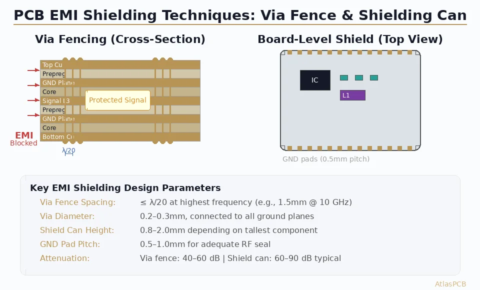
Via stitching: Complement edge plating with a row of ground vias along the board perimeter, spaced at λ/20 of the highest frequency of concern. For example, at 2.4 GHz (λ = 125mm), via spacing should be ≤ 6.25mm. Understanding [via design principles]/blog/pcb-via-types-guide/) is essential here.
Corner treatment: Inside corners of edge-plated perimeters tend to have thinner copper due to current distribution effects during electroplating. Add corner vias (within 1mm of each corner) to supplement the edge plating.
Layer count consideration: Edge plating effectiveness for EMI shielding improves with more ground layers. A 4-layer [stackup]/blog/pcb-stackup-design-guide/) with two ground planes provides better shielding than a 2-layer board because the ground cage has more continuous walls.
Edge Plating for RF and Microwave Applications
Waveguide and Cavity Grounding
In substrate-integrated waveguide (SIW) and cavity-backed antenna designs, edge plating provides the vertical walls of the waveguide structure:
- Via fence alternative: Edge plating can replace via fence walls in SIW designs, providing a truly continuous conductive wall instead of discrete via posts with gaps between them
- Insertion loss: Continuous edge plating reduces insertion loss by 0.1–0.3 dB/cm compared to via fence walls at frequencies above 10 GHz
- Cavity Q-factor: Edge-plated cavities achieve higher Q-factors (typically 1.5–2× improvement) compared to via-fenced cavities
Grounding for RF Shield Cans
When using soldered RF shield cans:
Edge plating as soldering surface: The plated edge provides a solderable surface for the shield can. Use ENIG or immersion tin [surface finish]/blog/pcb-surface-finish-guide/) for optimal solderability.
Thermal considerations: The shield can soldering process subjects the edge plating to localized temperatures of 260–300°C. Ensure copper adhesion testing covers this thermal profile.
Rework capability: Edge-plated connections allow shield can removal and replacement for debugging. Design the pad geometry to withstand 3× rework cycles without delamination.
Coplanar Waveguide Edge Grounding
For CPWG (Coplanar Waveguide with Ground) transmission lines near the board edge:
- Edge plating the board edge adjacent to a CPWG trace provides an additional ground reference, reducing radiation loss
- Maintain minimum 3× substrate thickness spacing between the CPWG signal trace and the plated edge to avoid impedance discontinuity
- For [impedance-controlled designs]/blog/pcb-impedance-control/), include the edge plating effect in the 2D field solver model
Surface Finish Options for Edge Plating
The surface finish applied to edge plating determines its solderability, corrosion resistance, and electrical performance:
| Surface Finish | Edge Plating Suitability | Key Characteristics |
|---|---|---|
| ENIG (Electroless Nickel / Immersion Gold) | Excellent | Best corrosion resistance; solderable; good for RF (low contact resistance) |
| HASL (Hot Air Solder Leveling) | Good | Solder coating on edges provides excellent solderability; uneven thickness |
| Immersion Tin | Good | Flat surface; good solderability; limited shelf life (6 months) |
| OSP (Organic Solderability Preservative) | Poor | Does not coat board edges reliably; not recommended for edge plating |
| Hard Gold (Electrolytic) | Excellent | Best wear resistance for connector edges; highest cost |
For castellated modules that will be soldered to carrier boards, ENIG is the recommended surface finish due to its excellent solderability, flat surface, and long shelf life (12+ months).
Testing and Quality Assurance
Visual Inspection (per IPC-A-600)
Edge plating is inspected per IPC-A-600 acceptance criteria:
- Class 3: No exposed substrate visible on plated edges at 10× magnification
- Plating must be continuous with no cracks or voids > 50μm
- Edge plating must contact all intended copper layers without bridging to unintended features
Cross-Section Analysis
Microsection analysis of edge-plated features should verify:
- Copper thickness ≥ 25μm at the thinnest point
- Good adhesion between plated copper and substrate at the routed edge
- Surface finish thickness within specification (e.g., ENIG: 3–5μm Ni, 0.05–0.1μm Au)
- No delamination between copper layers at the board edge
Electrical Testing
- Continuity: Verify edge plating connects top and bottom layers with resistance < 10mΩ
- Isolation: Verify minimum 500V isolation between edge plating and non-connected features
- EMI shielding effectiveness: For shielding applications, measure SE (Shielding Effectiveness) per IEEE 299 or MIL-STD-285. Target: ≥ 40dB at frequencies up to 3 GHz for typical applications
Common Edge Plating Design Mistakes
Mistake 1: Power Planes Touching the Board Edge
If a power plane extends to a plated edge, it will be shorted to ground (assuming the edge plating connects to the ground plane). Always maintain 0.5mm minimum clearance between power planes and plated board edges.
Mistake 2: Inadequate Routing Tolerance
The routing process that creates the final board edge must be precisely controlled. If the router bit removes too much material, the edge plating becomes too thin or discontinuous. If too little material is removed, FR-4 substrate remains on the edge surface. Typical routing tolerance for edge-plated boards: ±0.1mm.
Mistake 3: Missing Via Stitching
Edge plating alone may not provide sufficient EMI shielding at high frequencies (> 5 GHz). The plated edge needs to be supplemented with a row of stitching vias along the perimeter to prevent resonant slots between the edge plating and internal ground planes. Refer to our [via reliability testing guide]/blog/pcb-via-reliability-testing/) for stitching via spacing recommendations.
Mistake 4: Wrong Surface Finish for Application
Using OSP (organic preservative) on edge-plated features is unreliable because the OSP chemistry doesn’t uniformly coat the routed edge surface. For solderable edges, use ENIG or immersion tin. For high-wear connector edges, use hard electrolytic gold.
Mistake 5: Incorrect Castellation Hole Placement
Castellation holes must be precisely centered on the board outline. A 0.2mm offset results in one side having a thin sliver of copper that breaks off during depanelization. Always verify hole-to-edge registration in your [Gerber files]/blog/pcb-gerber-files-guide/) before releasing to fabrication.
Design Checklist for Edge-Plated PCBs
Before submitting your design for fabrication, verify:
- All copper layers not intended to connect to edge plating have ≥ 0.5mm clearance from board edge
- Ground planes extend to within 0.1mm of board edge at plating locations
- Solder mask pulled back 0.15–0.25mm from plated edges
- Castellation holes centered on board outline (±0.1mm tolerance)
- Via stitching row placed along edge-plated perimeter (spacing ≤ λ/20)
- Surface finish specified for edge plating (ENIG recommended)
- Fab drawing includes edge plating specification with minimum copper thickness
- Keepout zones defined in all copper layers near plated edges
- Panel array designed with castellations on V-score or tab-route lines
- Cross-section inspection coupon included in panel design
Edge plating transforms a standard PCB into a three-dimensional electromagnetic structure. By following the IPC-6012 requirements, manufacturing guidelines, and design rules in this guide, you can achieve reliable edge-plated designs for EMI shielding, module interconnection, and RF grounding applications — from initial prototype through volume production.
Ready to start your project? Upload your Gerbers for a free engineering review, or talk to an engineer about your design requirements.
Further Reading
- [HDI PCB Design Guide: Stackup Rules, Via Structures & DFM Checklist]/blog/hdi-pcb-design-guide/)
- [PCB Manufacturer with Engineering Review: Why Human DFM Audit Matters]/blog/pcb-manufacturer-engineering-review/)
- [PCB Manufacturing Process: 15 Steps from Gerber to Finished Board]/blog/pcb-manufacturing-process-15-steps/)
- [ENEPIG vs ENIG: Which PCB Surface Finish for Your Design?]/blog/enepig-vs-enig/)
- [PCB Solder Mask: Types, Colors, and Functions Explained]/blog/pcb-solder-mask-guide/)
About AtlasPCB — We specialize in complex PCB manufacturing for HDI, RF, and high-reliability applications. Explore our impedance-controlled PCB manufacturing . Every order includes free engineering review. Get your quote.
Reviewed by AtlasPCB Engineering Team — IPC-certified manufacturing specialists with 15+ years of production experience in HDI, RF, and high-reliability PCB fabrication. Content based on factory floor data and real customer design reviews.
- edge-plating
- pcb-manufacturing
- emi-shielding
- grounding