· AtlasPCB Engineering · Engineering · 9 min read
Networking Switch PCB Design: High-Speed Signal Integrity, Material Selection, and Thermal Management
Engineering guide to designing PCBs for networking switches. Covers high-speed signal integrity for 25G/50G/100G+ interfaces, high-layer-count stackup strategy, low-loss material selection, and thermal management for data center switch applications.
Networking Switch PCB Design: High-Speed Signal Integrity, Material Selection, and Thermal Management
Networking switch PCBs are among the most demanding boards manufactured today. A single modern data center switch carries a 25.6 Tbps (or higher) switching ASIC with 256 to 512 high-speed SerDes lanes, each running at 25G NRZ, 50G PAM4, or 100G+ PAM4 signaling. Every one of those lanes must traverse the PCB with enough signal margin to achieve a bit error rate (BER) below 10⁻¹⁵ after forward error correction.
This guide covers the PCB-specific design challenges for networking switches: stackup architecture, material selection, signal integrity, power delivery, and thermal management. Whether you’re designing a top-of-rack data center switch or an enterprise campus aggregation platform, these engineering principles apply.
The Design Challenge: Why Networking Switches Push PCB Limits
A networking switch PCB must simultaneously solve multiple conflicting engineering problems:
| Challenge | Requirement | Impact on PCB |
|---|---|---|
| Hundreds of high-speed lanes | 256–512 SerDes at 25–112 Gbps each | 20–28 layers, dense routing |
| Low insertion loss | < 0.8–1.0 dB/inch at Nyquist | Low-loss material mandatory |
| Controlled impedance | 85–100 Ω differential ±10% | Tight dielectric control |
| High power delivery | 200–500W for switching ASIC | Heavy copper, decoupling strategy |
| Thermal dissipation | 300–500W total board power | Thermal vias, heatsink interface |
| Dense BGA breakout | 0.8–1.0 mm pitch, 2,500+ balls | HDI or back-drill required |
| EMI compliance | FCC/CE/CISPR Class A | Ground plane strategy, edge shielding |
| Cost sensitivity | High-volume production | Material and process optimization |
No other PCB application combines all these challenges at this intensity level.
Stackup Architecture for Networking Switches
Layer Count Selection
The layer count for a networking switch PCB is primarily determined by:
- SerDes lane count — Each differential pair needs a routing channel. With 256 lanes (512 traces), you need sufficient signal layers to route all pairs with adequate spacing.
- Power domains — Modern switch ASICs require 8–15 distinct voltage rails (core, I/O, SerDes, PLL, analog). Each domain needs plane area.
- Ground planes — Every signal layer needs an adjacent ground reference. More signal layers mean more ground planes.
Typical layer counts by switch class:
| Switch Class | Throughput | SerDes Lanes | Typical Layers |
|---|---|---|---|
| Enterprise access | 480G–960G | 24–48 | 14–18 |
| Enterprise aggregation | 1.6T–6.4T | 64–128 | 18–22 |
| Data center ToR | 12.8T–25.6T | 128–256 | 20–24 |
| Data center spine | 25.6T–51.2T | 256–512 | 24–28 |
| Next-gen spine | 51.2T+ | 512+ | 28–32 |
Recommended Stackup Strategy
For a 24-layer data center switch PCB, a proven stackup strategy follows this pattern:
Signal–Ground–Signal–Ground alternation with power planes distributed in the center:
| Layer Group | Layers | Function |
|---|---|---|
| Outer high-speed | L1 (Sig), L2 (GND), L3 (Sig), L4 (GND) | Top-side high-speed SerDes routing |
| Upper routing | L5 (Sig), L6 (GND), L7 (Sig), L8 (PWR) | Secondary routing + first power plane |
| Mid-stack power | L9 (GND), L10 (PWR), L11 (PWR), L12 (GND) | Power distribution core |
| Center symmetry | L13 (GND), L14 (PWR), L15 (PWR), L16 (GND) | Mirrored power distribution |
| Lower routing | L17 (PWR), L18 (Sig), L19 (GND), L20 (Sig) | Secondary routing + power |
| Outer high-speed | L21 (GND), L22 (Sig), L23 (GND), L24 (Sig) | Bottom-side high-speed routing |
Key principles:
- L1/L3 and L22/L24 carry the highest-speed SerDes lanes between solid ground planes
- Power planes are concentrated in the center for structural symmetry
- Every signal layer has an adjacent ground reference
For a deeper dive into general [multilayer PCB stackup principles]/blog/multilayer-pcb-stackup-design-guide/), see our dedicated guide. For specific guidance on [impedance control methodology]/blog/pcb-impedance-control/), follow the link.
Material Selection for High-Speed Networking
Material choice is the single biggest factor determining whether a networking switch PCB can meet its insertion loss budget. Here’s the systematic approach:
Understanding the Loss Budget
Total channel loss from transmitter (TX) to receiver (RX) includes:
| Loss Component | Typical Contribution | PCB Design Influence |
|---|---|---|
| PCB dielectric loss | 40–60% of total | Material Df, trace length |
| PCB conductor loss | 15–25% of total | Copper roughness, trace width |
| Connector loss | 10–20% per connector | Connector selection |
| Via transition loss | 5–10% per transition | Via design, back-drill |
| Package loss | 5–15% | IC package selection |
For a typical 25G NRZ link at 12.5 GHz Nyquist:
- Total loss budget: ~25–30 dB (before equalization)
- PCB allocation: ~15–20 dB (for 10–15 inches of trace)
- Required loss rate: ≤ 1.0 dB/inch at 12.5 GHz
Material Selection by Data Rate
| Per-Lane Rate | Signaling | Nyquist Freq | Max Df (@ 10 GHz) | Material Class |
|---|---|---|---|---|
| 10G | NRZ | 5 GHz | 0.020 | Standard FR-4 |
| 25G | NRZ | 12.5 GHz | 0.008 | Mid-loss |
| 50G | PAM4 | 13.28 GHz | 0.005 | Low-loss |
| 100G | PAM4 | 26.56 GHz | 0.003 | Ultra-low-loss |
| 200G | PAM4 | 53+ GHz | 0.002 | Ultra-low-loss / advanced |
Copper Roughness: The Hidden Loss Factor
Copper surface roughness contributes significantly to conductor loss at high frequencies. The three common foil types:
| Foil Type | Roughness (Rz) | Loss Impact at 25 GHz | Cost Impact |
|---|---|---|---|
| Standard (STD) | 8–12 µm | Baseline | Baseline |
| Reverse-treated (RTF) | 4–6 µm | –15% loss | +5–10% |
| Very-low-profile (VLP) | 2–3 µm | –25% loss | +10–15% |
| Hyper-very-low-profile (HVLP) | 1–2 µm | –35% loss | +15–25% |
For 50G+ networking, VLP or HVLP foil is strongly recommended.

Signal Integrity Design Rules
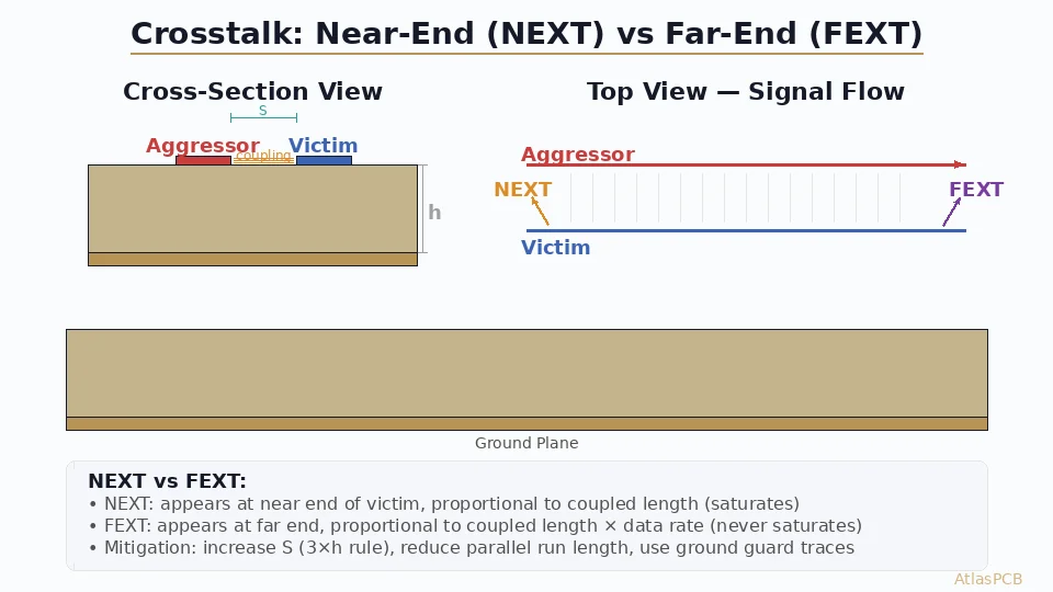
Differential Pair Routing
Networking switch PCBs route hundreds of differential pairs. Consistency is paramount:
| Parameter | 25G NRZ | 50G PAM4 | 100G PAM4 |
|---|---|---|---|
| Target impedance | 100 Ω diff (±10%) | 100 Ω diff (±8%) | 100 Ω diff (±7%) |
| Trace width | 4.0–5.0 mil | 3.5–4.5 mil | 3.0–4.0 mil |
| Pair spacing (edge-to-edge) | 5.0–6.0 mil | 4.5–5.5 mil | 4.0–5.0 mil |
| Pair-to-pair spacing | ≥ 4× dielectric height | ≥ 5× dielectric height | ≥ 5× dielectric height |
| Max intra-pair skew | ≤ 5 mil | ≤ 3 mil | ≤ 2 mil |
| Length matching tolerance | ±50 mil per group | ±25 mil per group | ±15 mil per group |
| Max via stubs | ≤ 10 mil | ≤ 8 mil | ≤ 5 mil |
Via Management
Via transitions are major loss contributors in high-speed networking PCBs. The management strategy includes:
Back-drilling (controlled-depth drilling):
- Remove via stubs to within 8 mil (200 µm) of the signal layer
- Required for all signals above 10 Gbps on boards thicker than 1.6 mm
- Back-drill diameter = via drill + 8 mil (minimum)
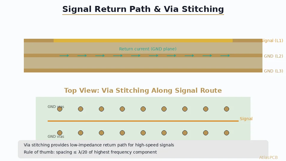
Ground return vias:
- Place ground stitching vias within 250 µm (10 mil) of every signal via
- Use at least 2 ground return vias per signal via transition
- This maintains return current path continuity across reference plane changes
Anti-pad optimization:
- Default anti-pad: via drill + 20 mil diameter
- For signal vias: optimize to minimize capacitance while maintaining clearance
- For ground vias on signal reference planes: minimize anti-pad to reduce impedance disruption
Glass Weave Skew Mitigation
At 50G+ signaling, glass fiber weave structure causes deterministic skew between the two traces of a differential pair. Standard E-glass 1080 weave can introduce 5–10 ps/inch of skew — enough to close the eye at 56 Gbps PAM4.
Mitigation approaches (from least to most aggressive):
- Routing angle: Route differential pairs at 5–15° to the glass weave direction
- Prepreg selection: Use spread-glass (NE-glass) or 1078/3313 styles
- Pair rotation: Periodically swap the P and N traces (requires careful impedance management)
- Material upgrade: Use PTFE-based or resin-coated-copper (RCC) dielectrics that eliminate glass entirely
For a complete treatment of [signal integrity principles in PCB design]/blog/signal-integrity-pcb-design-guide/), see our dedicated guide.
Power Delivery Network (PDN) Design
Power Requirements
A modern switching ASIC can draw 300–500W across multiple voltage domains:
| Voltage Rail | Typical Current | Rail Purpose |
|---|---|---|
| 0.75–0.85 V (core) | 200–400 A | Switch fabric core logic |
| 1.0–1.2 V (SerDes) | 50–100 A | High-speed transceiver banks |
| 1.8 V (I/O) | 10–30 A | General-purpose I/O |
| 3.3 V (management) | 5–10 A | Management CPU, PHYs |
| Various (PLL, analog) | 1–5 A each | Phase-locked loops, analog references |
PDN Design Strategy
Plane allocation:
- Dedicate 4–6 layers exclusively to power distribution
- Core voltage (highest current) gets the most plane area — ideally a full unbroken plane
- Use wide, short power delivery paths from VRM to ASIC
Decoupling strategy:
- Bulk capacitors: 100–470 µF aluminum electrolytic near VRM output
- Mid-frequency: 10–22 µF MLCC, distributed around ASIC perimeter
- High-frequency: 0.1–1.0 µF MLCC, placed within BGA escape area
- Ultra-high-frequency: On-die capacitance (ASIC-dependent)
Target impedance:
Z_target = (V_core × ripple%) / (I_transient)
For a 0.8 V core with 3% ripple and 100 A transient: Z_target = (0.8 × 0.03) / 100 = 0.24 mΩ
Achieving sub-milliohm impedance from DC to 1 GHz requires careful plane design, capacitor placement, and via optimization.
Thermal Management
Heat Generation Landscape
| Component | Typical Power | Thermal Solution |
|---|---|---|
| Switching ASIC | 200–500 W | Heatsink + forced airflow |
| QSFP/OSFP modules | 5–15 W each (×32) | Module cage + shared airflow |
| VRM (voltage regulators) | 20–50 W total | Heatsink + thermal pads |
| PHY ICs | 5–15 W each | PCB thermal vias + local heatsink |
| Memory (TCAM) | 10–30 W | PCB thermal management |
PCB Thermal Design for the ASIC
The switching ASIC is the dominant heat source. PCB thermal design for the ASIC focuses on:
Thermal via array under the BGA thermal pad:
- Via diameter: 0.3 mm, copper-filled
- Via pitch: 1.0 mm grid
- Coverage: Entire thermal pad area
- Thermal resistance contribution: ~0.5–1.0°C/W (PCB only)
Heavy copper planes:
- Inner ground planes at 2 oz (70 µm) copper weight
- These planes act as lateral heat spreaders
Bottom-side thermal pad:
- Exposed copper pad on the bottom side directly below the ASIC
- Connected to the ASIC thermal pad via copper-filled thermal vias
- Interfaces with a bottom-side heatsink or chassis mounting surface
Thermal relief management:
- Thermal pads on power planes should NOT use thermal relief patterns
- Direct connections provide lower thermal resistance
- Thermal relief is only appropriate for hand-soldering pads
Airflow Considerations
Networking switches use front-to-back (or back-to-front) airflow. PCB layout must accommodate:
- Component placement aligned with airflow direction
- Tall components (capacitors, inductors) upstream of sensitive ICs
- Adequate spacing between hot components to avoid thermal stacking
- Heatsink fin orientation parallel to airflow
Manufacturing Considerations for Networking Switch PCBs
Fabrication Complexity
| Feature | Typical Specification |
|---|---|
| Layer count | 20–28 |
| Board thickness | 2.0–3.2 mm |
| Minimum trace/space | 3.5/3.5 mil (outer), 3.0/3.0 mil (inner) |
| Via technology | Through-hole + back-drill |
| Via drill | 0.2–0.3 mm mechanical |
| Back-drill stub | ≤ 8 mil (200 µm) |
| Material | Low-loss laminate, Dk ≤ 3.6 |
| Copper weight | 1 oz outer, 1–2 oz inner |
| Surface finish | ENIG or immersion silver |
| Impedance tolerance | ±8% (differential) |
Panel Utilization
Networking switch PCBs are large — typically 400×300 mm to 500×400 mm. Panel utilization directly affects cost:
- Standard panel size: 18” × 24” (457 × 610 mm) or 21” × 24” (533 × 610 mm)
- Many switch PCBs yield only 1–2 boards per panel
- Board outline optimization can significantly impact material cost
- Working with your [multilayer PCB manufacturer]/blog/multilayer-fr4-pcb-manufacturer/) early in the design phase helps optimize panel layout
Testing Requirements
| Test | Method | Acceptance Criteria |
|---|---|---|
| Impedance | TDR (Time Domain Reflectometry) | ±8% of target |
| Insertion loss | VNA (Vector Network Analyzer) | Per channel loss budget |
| Continuity | Flying probe or fixture | All nets open/short free |
| Isolation | Hi-pot testing | Per IPC-9252 |
| Cross-section | Microsection per IPC-6012 | Class 3 requirements |
| Back-drill quality | X-ray and microsection | Stub ≤ specified maximum |
Design Review Checklist for Networking Switch PCBs
Before releasing your networking switch PCB design:
- Insertion loss simulation completed for worst-case lanes
- Material Df verified at the actual Nyquist frequency (not just 1 GHz)
- Copper roughness model included in simulation (Hammerstad-Jensen or Huray)
- Via stub length after back-drill verified by simulation
- Ground return vias placed at every signal via transition
- Differential impedance verified by field solver with actual stackup
- Intra-pair skew within specification for all differential pairs
- PDN impedance simulation shows target met from DC to 1 GHz
- Thermal simulation confirms ASIC junction temperature within limits
- DFM review completed with fabrication partner
- Panel utilization optimized
Conclusion
Networking switch PCB design is a convergence of high-speed signal integrity, power delivery engineering, thermal management, and manufacturing process optimization. The PCB is not just a passive interconnect — it’s an active participant in the signal chain that directly determines whether the switch meets its performance targets.
The keys to success:
- Start with the loss budget — Material selection flows from the required insertion loss per inch at the Nyquist frequency
- Design the stackup for signal integrity first — Then fit power and thermal requirements around it
- Manage every via transition — Back-drill, ground return vias, and anti-pad optimization are non-negotiable
- Collaborate with your fabricator early — Networking switch PCBs push fabrication limits; early DFM engagement prevents late-stage redesigns
Ready to manufacture your networking switch PCB? Request a quote from our engineering team — we provide comprehensive DFM review, impedance modeling, and loss-budget verification as part of our quotation process for high-speed networking boards.
This guide is maintained by the AtlasPCB Engineering team and reflects current industry best practices for data center and enterprise networking switch PCB design. For project-specific guidance, contact our high-speed design support team.
Further Reading
- [PCB Design for GaN and SiC Power Devices: Thermal Management, Layout Rules, and Material Selection]/blog/pcb-design-gan-sic-power-devices-thermal-layout/)
- [mmWave PCB Material Selection: Rogers vs Megtron vs LCP for 5G and 6G Applications]/blog/mmwave-pcb-material-selection-rogers-megtron-lcp-5g-6g/)
- [Rogers PCB Fabrication: Material Sourcing, Lead Times & Quality Control]/blog/rogers-pcb-fabrication/)
- [HDI PCB Design for 5G Antenna Integration: Signal Integrity Challenges in Millimeter-Wave Applications]/blog/hdi-5g-antenna-integration-pcb-design/)
- [RF PCB Material Selection for Automotive Radar: Rogers vs PTFE Performance Analysis at 77-81 GHz]/blog/automotive-radar-pcb-materials-rogers-ptfe-analysis/)
- Rigid PCB Manufacturing
About AtlasPCB — We specialize in complex PCB manufacturing for HDI, RF, and high-reliability applications. Explore our RF and high-frequency PCB services, or get an impedance-controlled PCB manufacturing . Every order includes free engineering review. Get your quote.
Reviewed by AtlasPCB Engineering Team — IPC-certified manufacturing specialists with 15+ years of production experience in HDI, RF, and high-reliability PCB fabrication. Content based on factory floor data and real customer design reviews.
- networking switch pcb
- high speed pcb
- data center pcb
- signal integrity
- 25G Ethernet
- switch fabric