· AtlasPCB Engineering · Engineering · 11 min read
OSP vs ENIG vs Immersion Silver: How to Choose PCB Surface Finish for Lead-Free Assembly
A practical engineering guide comparing OSP, HASL, ENIG, immersion silver, and ENEPIG surface finishes for lead-free PCB assembly — covering solderability, shelf life, cost, and fine-pitch compatibility.
Choosing the right PCB surface finish is one of the most consequential decisions in the design-for-manufacturing process. The finish protects exposed copper pads from oxidation, ensures reliable solder joints during assembly, and can influence everything from component coplanarity to RF signal integrity. With lead-free assembly now the global standard under RoHS directives, the interaction between surface finish chemistry and SAC (tin-silver-copper) solder alloys demands careful engineering consideration.
This guide compares the five most common surface finishes — OSP, HASL (lead-free), ENIG, immersion silver, and ENEPIG — with practical selection criteria for different assembly scenarios.
Why Surface Finish Selection Matters More in Lead-Free Assembly
The transition from tin-lead (SnPb) to lead-free solder alloys fundamentally changed surface finish requirements. SAC305 (Sn96.5/Ag3.0/Cu0.5) melts at 217–220°C compared to 183°C for eutectic SnPb, meaning reflow peak temperatures increased from ~215°C to 245–250°C. This higher thermal exposure places greater stress on surface finish coatings.
Key differences in lead-free assembly include:
- Higher reflow temperatures degrade OSP and immersion silver coatings faster during multiple thermal cycles
- SAC alloys have different wetting characteristics — they wet slower than SnPb, making surface finish quality more critical for consistent solder joint formation
- Intermetallic compound (IMC) growth accelerates at higher temperatures, affecting long-term solder joint reliability
- Fine-pitch components (0.4mm and below) require exceptional surface coplanarity that only certain finishes can provide
Understanding these interactions is essential for selecting a finish that balances manufacturability, reliability, and cost.

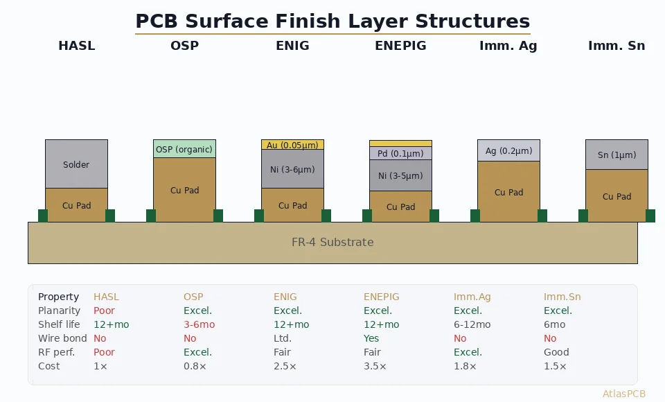
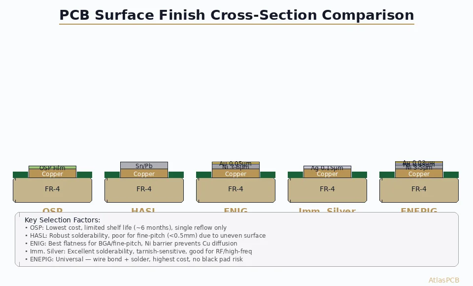
OSP (Organic Solderability Preservative)
OSP applies a thin organic film (typically benzimidazole or substituted benzimidazole compound) over bare copper to prevent oxidation. The coating is 0.2–0.5 μm thick and dissolves during the soldering process, leaving solder in direct contact with copper.
Advantages
- Lowest cost of any surface finish (typically 30–50% less than ENIG)
- Excellent solderability when fresh — direct copper-to-solder contact provides superior wetting
- Flat surface suitable for fine-pitch components
- Environmentally friendly — no heavy metals, simple chemistry
- Easy rework — the thin organic layer doesn’t interfere with rework processes
Limitations
- Limited shelf life — 6–12 months depending on formulation and storage conditions
- Degrades with thermal cycling — each reflow pass weakens the remaining coating
- Not suitable for multiple reflow applications without thicker formulations
- Difficult to inspect visually — transparent coating makes it hard to verify coverage
- ICT probe contact may be inconsistent after storage
Best Applications
OSP excels in high-volume consumer electronics with single-sided reflow, short supply chains (boards assembled within weeks of fabrication), and cost-sensitive applications where the BOM pressure demands the cheapest possible finish.
Lead-Free HASL (Hot Air Solder Leveling)
HASL dips the PCB into molten solder (typically SAC305 for lead-free) and uses hot air knives to level the coating. The result is a robust solder layer, typically 1–25 μm thick, that provides excellent solderability.
Advantages
- Proven reliability — decades of field history demonstrate excellent solder joint formation
- Long shelf life — the solder coating is inherently self-preserving; 12+ months is typical
- Excellent solderability even after extended storage
- Low cost (though more expensive than OSP)
- Multiple reflow compatible — the finish itself is solder, so thermal cycling has minimal effect
Limitations
- Uneven surface topology — the hot air leveling process cannot achieve perfect flatness, creating domed or irregular pad surfaces
- Not suitable for fine-pitch — components with pad pitch below 0.5mm (20 mil) may experience bridging or insufficient solder on smaller pads
- Thermal shock to bare board — the immersion in molten solder at ~260°C can stress the PCB, particularly thin boards or those with high aspect ratio vias
- Poor coplanarity — variations of 10–20 μm across a BGA footprint can prevent reliable simultaneous contact of all balls during placement
Best Applications
HASL remains an excellent choice for through-hole dominant boards, designs with pad pitches above 0.65mm, prototyping where shelf life flexibility is valuable, and military/aerospace applications where long-term solderability matters more than fine-pitch compatibility.
ENIG (Electroless Nickel / Immersion Gold)
ENIG deposits a nickel barrier layer (3–6 μm) over copper, followed by a thin immersion gold layer (0.05–0.1 μm). The gold prevents nickel oxidation during storage, and during soldering, tin from the solder alloy diffuses through the gold to form Ni₃Sn₄ intermetallic compounds with the nickel layer.
Advantages
- Exceptional coplanarity — the electroless process produces surface flatness within ±2 μm, ideal for BGA and fine-pitch components
- Excellent shelf life — 12+ months; the gold layer is highly resistant to oxidation
- Good for multiple reflow — the nickel barrier remains stable through 3–5 reflow cycles
- Wire bondable (aluminum wire) — suitable for certain chip-on-board applications
- Consistent ICT probe contact — the hard nickel surface provides reliable test points
Limitations
- Black pad defect — hyper-corrosion of the nickel layer during the immersion gold process can create a phosphorus-rich layer that inhibits solder wetting; this is the most significant ENIG reliability concern
- Higher cost — typically 2–3× the cost of OSP
- Nickel is magnetic — can interfere with magnetic sensors or certain RF applications
- Signal loss at high frequency — the nickel layer increases skin-effect losses above 1 GHz
- Brittle intermetallic — Ni₃Sn₄ is inherently more brittle than Cu₆Sn₅ formed with copper-based finishes
Best Applications
ENIG is the go-to finish for BGA-heavy designs, mixed-technology boards requiring fine-pitch and through-hole, [automotive PCBs]/blog/automotive-pcb-requirements/) where long shelf life and reliability are critical, and any design with pad pitch below 0.5mm.

Need Help Selecting the Right Surface Finish?
AtlasPCB supports ENIG, OSP, HASL, immersion silver, ENEPIG, and hard gold — with DFM review included on every order.
Get a Free QuoteImmersion Silver
Immersion silver deposits a thin layer of silver (0.15–0.4 μm) directly onto copper through a displacement reaction. The silver layer provides excellent solderability and the best electrical conductivity of any common surface finish.
Advantages
- Best RF/high-frequency performance — silver has the highest conductivity of any metal, minimizing insertion loss and skin-effect resistance
- Excellent coplanarity — suitable for fine-pitch and BGA components
- Good solderability — forms reliable Cu₆Sn₅ intermetallic (similar to OSP, since silver dissolves into the solder)
- Lower cost than ENIG — simpler chemistry with fewer process steps
- Lead-free compatible — no nickel barrier means no brittle Ni₃Sn₄ IMC
Limitations
- Tarnish sensitivity — silver readily reacts with sulfur compounds in the atmosphere, forming dark silver sulfide
- Shorter shelf life than ENIG — 6–12 months with proper packaging; significantly less in polluted environments
- Micro-voiding potential — some studies show higher micro-void rates in solder joints compared to ENIG
- Handling sensitivity — fingerprints and moisture accelerate tarnishing; gloves are mandatory
- Not suitable for press-fit connectors — the soft silver layer may be damaged during insertion
Best Applications
Immersion silver is the preferred finish for [RF and microwave PCBs]/blog/rf-microwave-pcb-design/), high-speed digital designs where signal integrity is paramount, [controlled impedance boards]/blog/controlled-impedance-pcb-design-stackup-calculations/) operating above 5 GHz, and membrane switch applications.
ENEPIG (Electroless Nickel / Electroless Palladium / Immersion Gold)
ENEPIG adds a palladium layer (0.05–0.1 μm) between the nickel and gold in the ENIG stack. This palladium layer acts as an additional barrier that prevents the gold from attacking the nickel, virtually eliminating the black pad defect.
Advantages
- Universal finish — supports both soldering and wire bonding (gold, aluminum, and copper wire) on the same board
- No black pad risk — the palladium barrier prevents nickel hyper-corrosion
- Excellent shelf life — 12+ months with robust oxidation protection
- Fine-pitch compatible — electroless deposition ensures excellent coplanarity
- Multiple reflow capable — stable through 5+ reflow cycles
Limitations
- Highest cost — 3–5× the cost of OSP; the palladium chemistry is expensive
- Complex process control — three separate deposition baths require tight parameter management
- Limited availability — fewer fabricators offer ENEPIG compared to ENIG or OSP
- Same RF concerns as ENIG — the nickel layer still introduces high-frequency losses
Best Applications
ENEPIG is essential for [mixed wire-bond and SMT designs]/blog/enepig-vs-enig-surface-finish-wire-bonding/), system-in-package (SiP) modules, automotive and medical devices where the highest reliability is required, and any application where black pad risk is unacceptable.
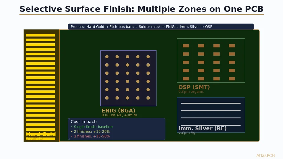
Surface Finish Selection Matrix
When selecting a surface finish, the decision tree typically follows this logic:
Step 1: Component requirements — Does the design include BGA with pitch ≤0.5mm? If yes, eliminate HASL. Does it require wire bonding? If yes, use ENEPIG (or ENIG for aluminum wire only).
Step 2: Frequency requirements — Is the design operating above 5 GHz? If yes, prefer immersion silver or OSP. The nickel layer in ENIG and ENEPIG increases losses.
Step 3: Assembly complexity — How many reflow passes are needed? Single reflow allows OSP. Double-sided reflow with fine-pitch on both sides needs ENIG or ENEPIG.
Step 4: Supply chain — How long between fabrication and assembly? Short supply chains (≤3 months) can use OSP or immersion silver. Long supply chains need ENIG or ENEPIG.
Step 5: Cost constraints — If the above steps allow multiple options, choose the lowest-cost finish that meets all requirements.
Real-World Selection Examples
Example 1: Consumer IoT Sensor Module
A Wi-Fi-connected temperature sensor with a QFN-48 (0.5mm pitch) microcontroller and 2.4 GHz antenna trace. Volume: 100,000 units/year.
Choice: OSP. The 0.5mm pitch is at the boundary but workable with OSP’s flat surface. Single reflow, short supply chain, and high volume make OSP’s cost advantage significant. The 2.4 GHz antenna benefits from no nickel layer.
Example 2: Automotive Radar Module
A 77 GHz FMCW radar with BGA radar transceiver, [Rogers RT/duroid substrate]/blog/automotive-radar-pcb-materials-rogers-ptfe-analysis/), and controlled impedance traces. Shelf life requirement: 18 months.
Choice: Immersion silver. The 77 GHz operating frequency makes nickel-based finishes unacceptable. Immersion silver’s superior conductivity minimizes trace losses. Vacuum-sealed storage extends shelf life to meet the 18-month requirement.
Example 3: Medical Implant Controller
A pacemaker controller board with 0.4mm pitch BGA, gold wire bonds for die attach, and IPC Class 3 reliability requirements. Must survive 2000 thermal cycles.
Choice: ENEPIG. The combination of BGA soldering and wire bonding on the same board makes ENEPIG the only viable option. The palladium barrier eliminates black pad risk for this life-critical application, and the robust layer stack survives extended thermal cycling. For more on medical device requirements, see our guide on [medical PCB manufacturing standards]/blog/medical-device-pcb-standards/).
Process Compatibility with Lead-Free Reflow
All five finishes are compatible with standard SAC305 reflow profiles (peak 245–250°C), but their behavior during reflow differs:
| Finish | Peak Temp Tolerance | Multiple Reflow | Wetting Speed |
|---|---|---|---|
| OSP | 260°C (degrades) | 1–2 passes | Fast |
| HASL | 260°C | 3+ passes | Fast |
| ENIG | 260°C | 3–5 passes | Moderate |
| Imm. Ag | 260°C (tarnish risk) | 2–3 passes | Fast |
| ENEPIG | 260°C | 5+ passes | Moderate |
The wetting speed difference matters for wave soldering and selective soldering processes where solder contact time is limited. OSP and immersion silver wet faster because tin interacts directly with copper (or copper through dissolved silver), while ENIG and ENEPIG require tin to first dissolve through the gold before reacting with nickel.
IPC Standards for Surface Finish
Several IPC standards govern surface finish specifications:
- IPC-4552 — Performance specification for ENIG
- IPC-4553 — Performance specification for immersion silver
- IPC-4554 — Performance specification for immersion tin
- IPC-4556 — Performance specification for ENEPIG
- IPC J-STD-003 — Solderability tests for printed boards (covers all finishes)
These specifications define minimum thickness requirements, solderability test methods, and acceptance criteria that ensure consistent quality across suppliers. When specifying surface finish in your fabrication drawing, reference the applicable IPC specification to avoid ambiguity.
Cost Comparison and Total Cost of Ownership
The raw finish cost per square foot typically ranks: OSP < HASL < Imm. Silver < ENIG < ENEPIG. However, total cost of ownership must consider:
- Scrap rate — HASL on fine-pitch designs increases defect rates, offsetting its lower finish cost
- Storage costs — OSP’s shorter shelf life may require more frequent orders and tighter inventory management
- Rework rate — black pad defects on ENIG boards create expensive rework scenarios in high-reliability applications
- Yield at assembly — the right finish for the component mix directly impacts first-pass yield
For most designs, the surface finish cost is less than 5% of the total board cost, but its impact on assembly yield and field reliability is disproportionately large. Selecting based solely on finish price is rarely the optimal strategy.
Conclusion
Surface finish selection is a systems-level decision that must account for component requirements, operating frequency, assembly process, supply chain timeline, and reliability targets. There is no universally “best” finish — only the best finish for a specific application.
For engineering teams unsure about the right choice, consider prototyping with multiple finishes using the same design to compare assembly results directly. Most PCB fabricators can provide split-lot production with different finishes on the same panel.
Ready to discuss surface finish options for your next project? AtlasPCB’s engineering team reviews every order for DFM compatibility, including surface finish selection for your specific component mix and assembly process. Request a quote and our engineers will recommend the optimal finish for your design.
Further Reading
- [ENEPIG vs ENIG: Surface Finish Selection for Wire Bonding Applications]/blog/enepig-vs-enig-surface-finish-wire-bonding/)
- [ENIG Surface Finish: Process, Specifications, and Black Pad Prevention]/blog/enig-surface-finish-process/)
- [PCB Surface Finish Guide: Complete Comparison for 2026]/blog/pcb-surface-finish-guide/)
- [Common PCB Defects and Prevention Strategies]/blog/common-pcb-defects-prevention/)
About AtlasPCB — We specialize in complex PCB manufacturing for HDI, RF, and high-reliability applications. Explore our RF and high-frequency PCB services, or get an full PCB manufacturing capabilities . Every order includes free engineering review. Get your quote.
Reviewed by AtlasPCB Engineering Team — IPC-certified manufacturing specialists with 15+ years of production experience in HDI, RF, and high-reliability PCB fabrication. Content based on factory floor data and real customer design reviews.
- surface finish
- ENIG
- OSP
- HASL
- immersion silver
- ENEPIG
- lead-free assembly
- solderability
- PCB manufacturing