· AtlasPCB Engineering · Engineering · 8 min read
OSP vs HASL vs ENIG: How to Choose the Right PCB Surface Finish (2026 Decision Guide)
Can't decide between OSP, HASL, and ENIG for your PCB? This decision guide gives you the answer in 30 seconds based on your design requirements, budget, and assembly process.
The 30-Second Answer
Don’t have time for the full breakdown? Here’s the decision in one table:
| Your Design Situation | Best Finish | Reason |
|---|---|---|
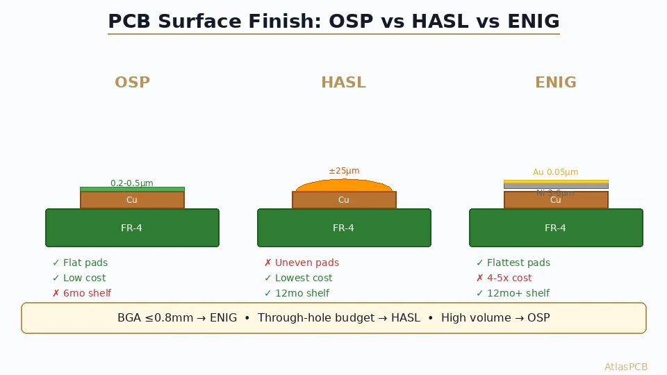
| Fine-pitch BGA (≤0.8mm) | ENIG | Flat pads prevent solder bridging |
| Wire bonding / gold wire | ENIG | Gold-to-gold bond reliability |
| Budget prototype, through-hole | HASL | Cheapest, most forgiving |
| High-volume consumer (>50k/yr) | OSP | Lowest cost at scale |
| Mixed SMD + through-hole | ENIG | Best all-around for complex boards |
| Long shelf life (>6 months) | ENIG | 12+ month shelf life |
| RF / microwave | ENIG or Imm. Silver | Consistent impedance |
Rule of thumb: If you have ANY BGA with pitch ≤0.8mm, choose ENIG. If you don’t, you can save money with HASL or OSP.
How Each Finish Works (Cross-Section)
Understanding the physical structure helps you understand the tradeoffs:
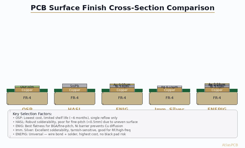
OSP (Organic Solderability Preservative) A thin organic layer (0.2–0.5μm) applied chemically to bare copper. Think of it as a transparent shield that prevents oxidation until soldering.
HASL (Hot Air Solder Leveling) The board is dipped in molten solder, then hot air knives blow off the excess. This creates a dome-shaped solder coating (1–25μm) on each pad — robust but inherently uneven.
ENIG (Electroless Nickel Immersion Gold) A two-layer system: 3–6μm electroless nickel provides the structural barrier, topped by 0.05–0.1μm immersion gold that prevents nickel oxidation. Results in perfectly flat, solderable pads.
Cost Comparison (Real Numbers)
Let’s talk money. Here’s what each finish actually costs on a typical 4-layer, 100×160mm board:
| Surface Finish | Added Cost/Panel | vs. Baseline | Break-Even Volume |
|---|---|---|---|
| OSP | $2–4 | 1x (baseline) | Always cheapest |
| HASL (leaded) | $3–5 | ~1.3x | — |
| HASL (lead-free) | $4–7 | ~1.7x | — |
| ENIG | $12–20 | 4–5x | — |
| Immersion Silver | $8–14 | 3x | — |
Key insight: On a $200 prototype order, the difference between OSP and ENIG is about $15–30. Don’t let surface finish cost drive your prototype decisions — it’s negligible. Cost optimization matters at 10,000+ panels/year.
INSTANT QUOTE
Need an Exact Price for Your Design?
Upload Gerber files and compare all surface finish options side-by-side. No commitment.
Compare Prices ›Technical Specifications (Head-to-Head)
Pad Flatness & Fine-Pitch Capability
This is where the three finishes diverge most dramatically:
| Parameter | OSP | HASL | ENIG |
|---|---|---|---|
| Pad flatness | ±5μm Yes | ±25μm Caution | ±5μm Yes |
| Min pad pitch | 0.4mm | 0.65mm | 0.3mm |
| BGA compatible | Yes (≥0.5mm) | No (>0.8mm only) | Yes (all pitches) |
| Wire bondable | No | No | Yes |
| Press-fit ready | Marginal | No | Yes |
Shelf Life & Reflow Tolerance
| Parameter | OSP | HASL | ENIG |
|---|---|---|---|
| Shelf life (sealed) | 6 months | 12 months | 12+ months |
| Shelf life (open) | 24–48 hours Caution | 6+ months | 12+ months |
| Max reflow cycles | 2–3 | 3–4 | 6+ |
| N₂ atmosphere needed | Recommended | No | No |
| Lead-free compatible | Yes | Yes (Pb-free alloy) | Yes |
Electrical & Reliability
| Parameter | OSP | HASL | ENIG |
|---|---|---|---|
| Solder wetting | Good (when fresh) | Excellent | Excellent |
| ICT probe contact | Good | Excellent | Excellent |
| Contact resistance | Low | Low | Lowest |
| Impedance impact | None | Pad dome affects Z₀ | Minimal (+5μm Ni) |
| Corrosion resistance | Low | High | Highest |
Failure Modes: What Goes Wrong
OSP Failures
The #1 OSP failure: pad oxidation from storage. If your boards sit for more than a few days in humid conditions without sealed packaging, the organic layer breaks down and copper oxidizes underneath.
Symptoms:
- Dark/discolored pads
- Poor solder wetting (solder balls, dewetting)
- Higher defect rates on second reflow pass
Prevention: Vacuum-sealed packaging with desiccant. Use within 48h of opening. Consider ENIG if your supply chain has any delay.
HASL Failures
The #1 HASL failure: solder bridging on fine-pitch pads. The uneven dome height (±25μm) means adjacent pads on a 0.5mm-pitch BGA can literally touch with solder.
Symptoms:
- Bridging on BGA/QFN after reflow
- Tombstoning on 0201/0402 passives (uneven pad height)
- Board warpage on thin panels (<1.0mm) from thermal shock during HASL process
Prevention: Don’t use HASL if your finest pitch is below 0.65mm. Period.
ENIG Failures
The #1 ENIG failure: black pad syndrome. A nickel corrosion defect that creates a dark, phosphorus-rich layer between nickel and gold, causing brittle solder joints that can fail months after assembly.
Symptoms:
- Dark/black appearance on pads after gold strip
- Brittle fracture at pad interface under stress
- Random open joints discovered in field returns
Prevention: Specify mid-phos nickel (7–9% P), gold ≤0.1μm, and ensure your fab monitors bath chemistry. At AtlasPCB, we replace nickel bath at 6 metal turnovers (industry standard: 8) — our black pad rate is <0.01%.
FREE DFM REVIEW
We Catch Surface Finish Mismatches Before Production.
Upload your design — our engineers flag incompatible pads before fab starts. No charge.
Real-World Application Examples
Example 1: Bluetooth Earbuds (OSP Yes)
Design: 2-layer, 0.8mm thick, all 0402 passives + QFN BLE module (0.5mm pitch) Volume: 100,000 units/year Assembly: Single-sided SMD, boards assembled within 3 days of delivery
Why OSP works: Fast turnover eliminates shelf life concerns. Single reflow. Cost savings: $0.03/board × 100k = $3,000/year.
Risk: If production delays cause boards to sit >1 week, switch to ENIG.
Example 2: Industrial Motor Controller (HASL Yes)
Design: 4-layer, 1.6mm, TO-220 MOSFETs + screw terminals + 1206 passives Volume: 2,000 units/year Assembly: Mixed through-hole and SMD, hand-soldering for rework
Why HASL works: No fine pitch, excellent through-hole filling, rework-friendly. Boards may sit in inventory 6+ months — HASL handles that fine.
Risk: If you later add a BGA to the design, you’ll need to switch finishes.
Example 3: FPGA Carrier Board (ENIG Yes)
Design: 10-layer HDI, 0.5mm BGA + DDR4 + USB-C + press-fit backplane connector Volume: 500 units/year Assembly: Double-sided SMD + selective wave + press-fit
Why ENIG is the only option: 0.5mm BGA requires flat pads. Press-fit needs consistent surface. DDR4 impedance requires uniform geometry. No other finish qualifies.
Example 4: 5G mmWave Antenna (Immersion Silver )
Design: 2-layer Rogers 4350B, microstrip patch array, 28GHz Volume: 5,000 units/year
Plot twist: For RF above 10GHz, consider immersion silver instead of ENIG. The 5μm nickel layer in ENIG is ferromagnetic and introduces insertion loss at mmWave frequencies. Immersion silver provides flat pads with no magnetic interference.
Special Cases & Advanced Options
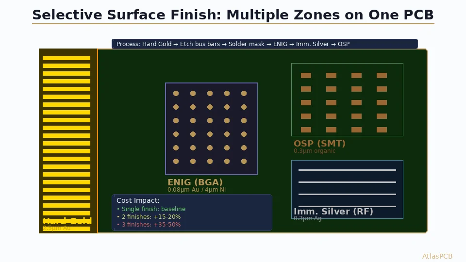
Selective Finish (Multiple Finishes on One Board)
You can combine finishes:
- ENIG + Hard Gold on edge connector fingers (most common combo)
- ENIG + OSP where BGA pads get ENIG but the rest gets OSP (cost optimization at volume)
This adds NRE cost ($50–200) but optimizes each area individually. Worth it above 1,000 panels/year.
When to Consider Immersion Silver or Tin
| Alternative | Use When | Advantage Over ENIG |
|---|---|---|
| Immersion Silver | RF/microwave, fine pitch on budget | No magnetic Ni layer, 40% cheaper |
| Immersion Tin | Press-fit connectors, automotive | No nickel = no black pad risk |
| ENEPIG | Wire bonding + soldering on same board | Al & Au wire bondable |
Assembly Compatibility Matrix
If your design goes through multiple assembly processes, this matters:
| Assembly Process | OSP | HASL | ENIG | Notes |
|---|---|---|---|---|
| Single reflow (top) | Yes | Yes | Yes | All work |
| Double reflow (top + bottom) | Caution | Yes | Yes | OSP degrades on 2nd pass |
| Wave solder | Yes | Yes | Yes | All work |
| Selective solder | Yes | Caution | Yes | HASL dome interferes with selective nozzle |
| Press-fit | No | No | Yes | Only ENIG or hard gold |
| Wire bonding | No | No | Yes | Only ENIG or ENEPIG |
| Hand rework | Caution | Yes | Yes | OSP oxidizes on exposed pad |
ENGINEERING REVIEW
Not Sure Which Finish Your Design Needs?
We analyze your Gerber files, BOM, and assembly process — then recommend the optimal finish. Our engineers review your design before production.
Get Recommendation ›IPC Standards Reference
For your fab drawing, here are the relevant specs:
| Standard | What It Covers |
|---|---|
| IPC-4552A | ENIG specification (Ni: 3–6μm, Au: 0.05–0.15μm) |
| IPC-4553A | Immersion silver requirements |
| IPC-4554 | Immersion tin requirements |
| IPC-4555 | ENEPIG specification |
| J-STD-003 | Solderability testing for surface finishes |
What to specify in your fab notes:
Surface Finish: ENIG per IPC-4552A Class 1
Nickel: 3-6μm electroless, mid-phosphorus (7-9% P)
Gold: 0.05-0.10μm immersion
Making Your Final Decision
The Engineering Flowchart
- Any BGA ≤0.8mm pitch? → ENIG. Stop here.
- Wire bonding required? → ENIG (or ENEPIG for aluminum wire). Stop.
- Press-fit connectors? → ENIG on those pads (selective OK). Stop.
- RF above 10GHz? → Immersion silver. Stop.
- Volume >50k/year AND fast assembly (<1 week)? → OSP. Stop.
- Everything else? → HASL for budget, ENIG for safety.
Cost-Conscious Engineer’s Cheat Sheet
- Prototype: Just use ENIG. The $15 premium isn’t worth the risk of choosing wrong.
- Low volume (100–5,000/yr): ENIG unless purely through-hole → then HASL.
- High volume (>10k/yr): Run the numbers. OSP saves $0.02–0.05/board. Over 100k boards, that’s real money.
- Qualification boards: Always ENIG. Don’t let surface finish variability confound your test results.
Conclusion
Surface finish selection comes down to three questions:
- What’s your finest pitch? (Determines if you MUST use ENIG)
- What’s your shelf life requirement? (Eliminates OSP if >6 months)
- What’s your annual volume? (Determines if cost optimization matters)
For 80% of designs today, ENIG is the right answer. It’s the safe, reliable choice that works with everything. Only deviate from ENIG if you have a specific reason — and now you know exactly what those reasons are.
ATLASPCB
Ready to Order? Quote in 60 Seconds.
All surface finishes available. Prototype in 48 hours. Engineering review available on every order.
Get Instant Quote ›Related Reading:
About AtlasPCB — We specialize in complex PCB manufacturing for HDI, RF, and high-reliability applications. Explore our RF and high-frequency PCB services, or get an free engineering DFM review . Every order includes free engineering review. Get your quote.
Reviewed by AtlasPCB Engineering Team — IPC-certified manufacturing specialists with 15+ years of production experience in HDI, RF, and high-reliability PCB fabrication. Content based on factory floor data and real customer design reviews.
- surface-finish
- pcb-manufacturing
- dfm
- cost-optimization