· AtlasPCB Engineering · Engineering · 8 min read
Thermal Shock Testing and IST for PCB Reliability: IPC-TM-650 Methods, Failure Modes, and Pass Criteria
Complete guide to PCB thermal shock testing and Interconnect Stress Testing (IST) per IPC-TM-650 standards. Learn test methods, cycle parameters, failure mechanisms, pass/fail criteria, and when to specify each test for via reliability qualification.
Introduction: Why PCB Reliability Testing Matters
A PCB may pass all electrical tests at room temperature on Day 1 — yet fail catastrophically after three months in the field. The difference between a board that works on the bench and one that survives 10 years of thermal cycling in an automotive engine bay or satellite orbit comes down to interconnect reliability — specifically, the integrity of plated through-holes and microvias under thermomechanical stress.
Two test methods dominate PCB reliability qualification:
- Thermal Shock Testing (IPC-TM-650 2.6.7.2) — the traditional approach using external temperature chambers
- Interconnect Stress Testing (IST) (IPC-TM-650 2.6.26) — a newer, faster method using internal resistive heating
Both methods answer the same fundamental question: Will the copper interconnects survive repeated thermal expansion without cracking? But they differ significantly in speed, sensitivity, cost, and applicability.
The Physics of Via Failure
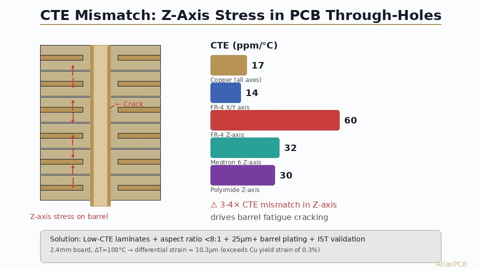
Understanding why vias fail under thermal cycling requires knowledge of one critical material property: the Coefficient of Thermal Expansion (CTE) mismatch between copper and FR-4.
| Material | CTE (ppm/°C) | Direction |
|---|---|---|
| Copper | 17 | All directions (isotropic) |
| FR-4 (X-Y plane) | 12-16 | In-plane (constrained by glass) |
| FR-4 (Z-axis) | 50-70 | Through-thickness (resin-dominated) |
When the board heats up, the FR-4 substrate expands approximately 3-4× faster in the Z-axis than the copper barrel inside the via. This differential expansion creates tensile stress on the copper plating — pulling it apart from the inside.
The Fatigue Mechanism
Each thermal cycle:
- Heating: substrate expands, stretching the copper barrel
- Dwell at temperature: stress relaxation (copper creeps slightly)
- Cooling: substrate contracts, copper returns to neutral state
- Repeat: each cycle accumulates fatigue damage
After enough cycles, a fatigue crack initiates at the highest-stress point — typically the via knee (the corner where the barrel wall transitions to the surface capture pad). The crack propagates inward with each cycle until it separates the barrel into disconnected segments, creating an electrical open.
High-Risk Geometries
Certain via configurations fail faster:
- High aspect ratio (board thickness ÷ drill diameter > 8:1) — more copper length under stress
- Thin plating (< 20 μm average, < 18 μm minimum) — less copper to resist cracking
- Plating voids — stress concentrators that nucleate cracks
- Via-in-pad without proper fill — thermal stress concentrates at void boundaries
- Lead-free assembly — higher reflow temperatures (260°C peak) create initial grain damage
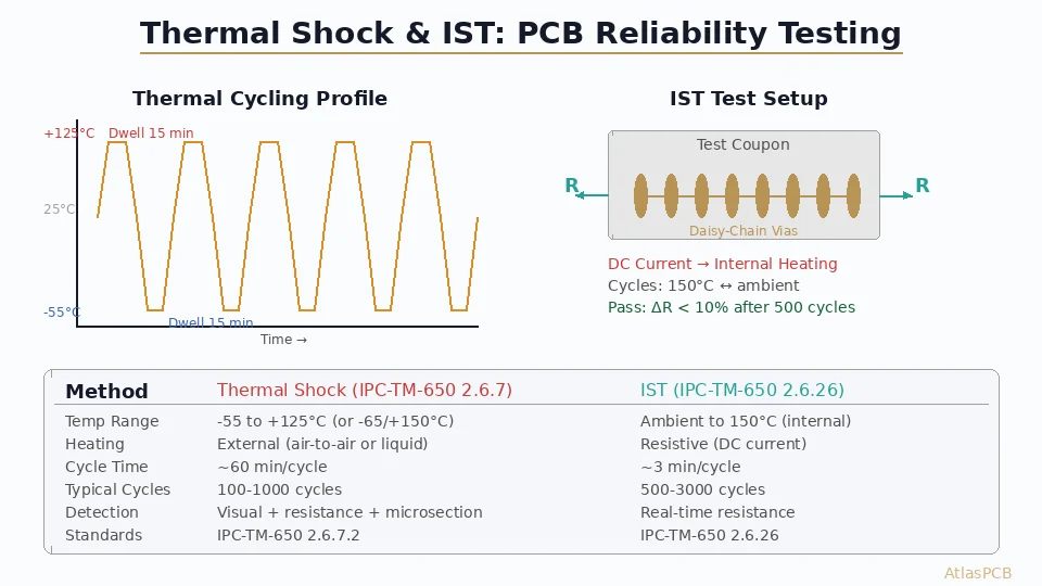
Thermal Shock Testing (IPC-TM-650 2.6.7.2)
Method Overview
Thermal shock testing exposes PCB test coupons to rapid temperature cycling between two extreme chambers. The “shock” comes from the fast transition — the coupon moves from hot to cold (or vice versa) in under 60 seconds, not allowing the copper to gradually accommodate strain.
Test Parameters
| Parameter | Condition A | Condition B | Condition C |
|---|---|---|---|
| High temperature | +125°C | +100°C | +150°C |
| Low temperature | -55°C | -40°C | -65°C |
| Dwell time (each extreme) | 15 min | 10 min | 15 min |
| Transfer time | < 60 sec | < 60 sec | < 60 sec |
| Total cycle time | ~60 min | ~45 min | ~60 min |
| Typical cycles | 100-1000 | 200-500 | 100-500 |
Condition A (-55°C to +125°C) is the most common for commercial and industrial PCBs. Condition C (-65°C to +150°C) is used for extreme-environment applications (military, automotive under-hood, space).
Equipment Types
- Air-to-Air chambers — two-zone ovens with automated transfer mechanism. Slower but simpler.
- Liquid-to-liquid (Fluorinert™) — direct immersion provides faster heat transfer and more severe thermal shock. Used for accelerated testing.
Monitoring During Test
- Resistance measurement — continuous or per-cycle monitoring of daisy-chain circuits
- Event detection — automated systems flag any resistance increase > 10% threshold
- Interim microsection — destructive cross-section analysis at cycle intervals (e.g., 100, 300, 500 cycles)
Pass/Fail Criteria
Per IPC-6012 Class 3:
- ΔR < 10% after specified cycle count
- No visible barrel crack in microsection
- No corner crack > 50% of plating thickness
- No interconnection separation at internal layers
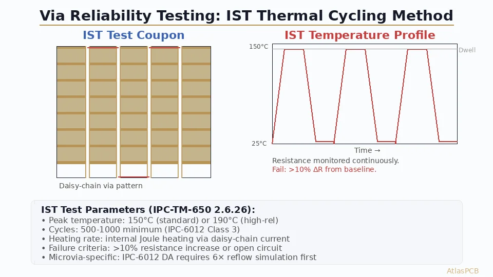
Interconnect Stress Testing (IST) — IPC-TM-650 2.6.26
How IST Works
IST uses a fundamentally different heating mechanism: instead of external temperature chambers, IST passes DC current through the copper traces and vias of a test coupon, heating the board from the inside out through I²R (Joule) heating.
The process:
- Heating phase — current flows through the daisy-chain circuit, heating the copper to ~150°C (measured by resistance increase)
- Cooling phase — current stops, forced air or natural convection cools the coupon to ambient
- Resistance measurement — precise 4-wire measurement at room temperature before and after each cycle
- Cycle time — approximately 3 minutes per complete thermal cycle
Why IST Is Faster
| Parameter | Thermal Shock | IST |
|---|---|---|
| Cycle time | 45-60 min | 3 min |
| Cycles per day | 20-30 | 400-500 |
| Time to 500 cycles | 2-3 weeks | ~1 day |
| Sample quantity | Limited by chamber size | 1-4 coupons per channel |
| Capital cost | $50K-200K (chambers) | $30K-50K (IST system) |
IST completes a 500-cycle reliability qualification in 24 hours versus 2-3 weeks for thermal shock. This speed enables:
- Rapid process development iteration
- Incoming material qualification
- Production lot sampling
- Supplier evaluation programs

High-Reliability PCB Manufacturing with IST Qualification
AtlasPCB maintains IST-qualified processes for IPC Class 3 multilayer and HDI boards. Every production lot includes reliability coupon data.
View Our Capabilities →IST Coupon Design
IST requires a dedicated test coupon with specific features:
- Daisy-chain pattern — vias connected in series (plated through-holes only — not via-in-pad with fill)
- Separate heating and sensing circuits — 4-wire Kelvin measurement eliminates lead resistance errors
- Multiple via configurations — different drill sizes, aspect ratios, and layer connections on one coupon
- Reference resistor — an on-coupon trace of known geometry for temperature calibration
Standard IST coupons include:
- Through-via daisy chain (full board thickness)
- Blind via chain (if HDI)
- Stacked microvia chain (if applicable)
- Thermal pad chain (for power plane connections)
IST Pass/Fail Criteria
The standard pass criterion is:
- ΔR < 10% after the specified number of cycles
- Typical Class 3 requirement: ≥ 150 cycles without exceeding 10% resistance change
- Aggressive requirements (aerospace): ≥ 300 cycles (some programs require 500+)
The 10% threshold correlates to the onset of barrel fatigue cracking as confirmed by microsection analysis. A 5% resistance increase typically indicates micro-cracking has begun but circuit continuity is maintained.
When to Specify Each Method
Use Thermal Shock When:
- Customer specification requires it (MIL-PRF-31032, NASA-STD-8739.4)
- Testing solder joint reliability (not just via barrels) — thermal shock stresses joints directly
- Board-level assembly qualification (populated PCBAs)
- Need to capture assembly defects (cold joints, cracked joints)
Use IST When:
- Qualifying bare board interconnect reliability
- Rapid feedback needed during process development
- Supplier comparison testing (same coupon design, different suppliers)
- HDI microvia reliability qualification
- Production lot acceptance testing
- Cost-effective alternative when spec permits
Can They Replace Each Other?
IST does not replace thermal shock for solder joint testing — IST stresses via barrels only. Conversely, thermal shock tests solder joints AND via barrels simultaneously, but takes weeks and provides less via-specific diagnostic data.
For a complete reliability program:
- Use IST for via reliability qualification (fast, sensitive, low cost per cycle)
- Use thermal shock for assembly-level qualification (captures joint + via + component failure modes)
Design Guidelines for Reliability
Based on IST failure analysis data, here are design rules that maximize via reliability:
1. Plating Thickness
| Min. Average Plating | Min. at Knee | IPC-6012 Class |
|---|---|---|
| 20 μm | 18 μm | Class 2 (commercial) |
| 25 μm | 20 μm | Class 3 (high-reliability) |
| 30 μm | 25 μm | Best practice for >10:1 AR |
Specify copper plating uniformity requirements in your fabrication drawing. Plating thickness at the via knee is the critical measurement — not the mid-barrel average.
2. Aspect Ratio Limits
| Max Aspect Ratio | Recommended Application |
|---|---|
| 8:1 | Standard commercial |
| 10:1 | With enhanced plating process |
| 12:1 | Requires pulse-reverse plating |
| >12:1 | Not recommended for Class 3 |
Higher aspect ratios mean more z-axis copper under tensile stress. For aspect ratios above 10:1, consider back-drilling to reduce the effective via length and improve both signal integrity AND reliability.
3. Via Fill Quality
For VIPPO (Via-in-Pad Plated Over) structures, fill quality directly affects reliability:
- Dimple depth: < 10 μm (flat fill preferred)
- No voids visible in X-ray
- Fill material: electroplated copper (conductive) preferred over non-conductive paste for thermal reliability
4. Reflow Considerations
Each reflow cycle adds thermal damage:
- Limit total reflow passes to 2-3 maximum
- Peak temperature: lowest profile that achieves acceptable joints
- Optimize reflow profile to minimize time above liquidus
Failure Analysis After Testing
When test coupons fail, the investigation follows a standard sequence:
- Identify failure location — which via in the daisy chain shows maximum ΔR?
- Cross-section preparation — mount, grind, and polish through the suspect via
- Optical microscopy — identify crack location (knee, mid-barrel, inner-layer interface)
- SEM analysis — examine fracture surface morphology (fatigue striations vs. brittle fracture)
- Root cause determination — correlate failure mode with process variable
Common Failure Modes
| Failure Mode | Root Cause | Corrective Action |
|---|---|---|
| Knee crack (most common) | Thin plating at knee, CTE stress | Increase min. plating, reduce AR |
| Barrel fatigue crack | Insufficient plating thickness | Improve plating uniformity |
| Inner-layer separation | Poor oxide/bond treatment | Review inner-layer prep |
| Corner crack | Drill damage + thin plating | Optimize drill parameters |
| Via fill delamination | Poor fill adhesion, voiding | Qualify fill process |
Industry Trends
IST Adoption Growing
IST adoption has accelerated across the PCB industry over the past 5 years, driven by:
- HDI proliferation requiring rapid microvia qualification
- Automotive qualification timelines that can’t accommodate weeks of thermal shock
- Data-driven manufacturing requiring statistical process control on interconnect reliability
Major automotive OEMs (Continental, Bosch, ZF) now accept IST results in lieu of traditional thermal shock for bare-board qualification — significantly compressing qualification timelines from months to days.
In-Line IST Monitoring
Leading fabricators are implementing IST as an in-process control — testing coupons from every production lot rather than relying solely on periodic qualification. This approach catches process drift (plating thickness variation, solution contamination) before it reaches shipped product.
Conclusion
Thermal shock testing and IST are complementary tools for ensuring PCB interconnect reliability. The choice between them depends on what you’re qualifying (bare board vs. assembly), how fast you need results, and what your customer specification mandates.
For engineers designing high-reliability products, the key takeaway is: reliability is designed in, not tested in. Proper plating thickness, controlled aspect ratios, qualified materials, and minimized reflow exposure create robust interconnects that pass any test method — whether it takes 3 minutes or 3 weeks per cycle.
Need IST-qualified PCB manufacturing? AtlasPCB provides IPC Class 3 boards with IST reliability data included on every production lot. Learn about our capabilities →
Further Reading:
About AtlasPCB — We specialize in complex PCB manufacturing for HDI, RF, and high-reliability applications. Explore our aluminum and metal-core PCB services, or get an full PCB manufacturing capabilities . Every order includes free engineering review. Get your quote.
Reviewed by AtlasPCB Engineering Team — IPC-certified manufacturing specialists with 15+ years of production experience in HDI, RF, and high-reliability PCB fabrication. Content based on factory floor data and real customer design reviews.
- PCB reliability
- thermal shock
- IST
- IPC-TM-650
- via reliability
- thermal cycling
- interconnect stress test
- qualification