· AtlasPCB Engineering · News · 7 min read
Next-Gen AI Servers Are Pushing PCB Technology Toward Ultra-HDI Manufacturing
AI GPU clusters and networking switches demand sub-50μm traces, any-layer microvias, and 20+ layers — driving a manufacturing revolution in PCB fabrication.
AI’s Insatiable Appetite for Advanced PCBs
The artificial intelligence infrastructure buildout that has dominated the semiconductor industry since 2023 is now sending shockwaves through the PCB manufacturing sector. As GPU training clusters grow more powerful and networking switches push to higher radix counts, the printed circuit boards connecting these chips are being pushed to manufacturing limits that were, until recently, the exclusive domain of IC substrate fabrication.
The shift is not incremental. Current-generation AI server platforms from leading hyperscalers are already specifying PCB requirements that strain the capabilities of all but the most advanced fabrication shops: sub-50μm trace and space widths, any-layer [microvia interconnects]/blog/pcb-laser-drilling-microvia-technology/) stacked five or more levels deep, 20-30 layer stackups with tight impedance control across dozens of differential pairs, and copper-filled via structures that must survive thousands of thermal cycles without cracking.
This article examines what is driving these requirements, how PCB manufacturers are responding, and what it means for the broader industry.
What Makes AI Server PCBs Different
To understand why AI servers are pushing PCB technology so hard, it helps to examine the specific design challenges:
Massive BGA Escape Routing
Modern AI GPUs — the chips at the heart of training clusters — come in BGA packages measuring 60-80mm per side with ball counts exceeding 5,000. At ball pitches of 0.8mm and trending toward 0.65mm, escaping all those signals through the PCB requires trace widths and spaces below 50μm. Traditional subtractive etching processes, which form traces by removing unwanted copper, struggle below 75μm due to etch undercut. This is driving adoption of the [modified semi-additive process (mSAP)]/news/msap-process-adoption-pcb-industry-2026/), which builds traces up from a thin seed layer to achieve finer features.
High-Speed Signal Integrity Demands
AI servers don’t just need dense routing — they need it with exceptional signal integrity. A single AI server motherboard may carry:
- PCIe Gen6 at 64 GT/s (PAM4) connecting GPU to CPU
- NVLink or proprietary chip-to-chip links at 100+ Gbps per lane
- HBM interfaces with thousands of parallel data lines
- Ethernet at 400G-800G for network fabric connectivity
Each of these interfaces demands [controlled impedance]/blog/pcb-impedance-control/) routing with tight tolerances (typically ±5%), minimal insertion loss, and carefully managed return paths. The combination of fine traces and high-speed requirements pushes [material selection]/blog/pcb-high-speed-material-dk-df-comparison/) toward ultra-low-loss laminates — the same types of materials traditionally reserved for RF and microwave applications.
Layer Count Escalation
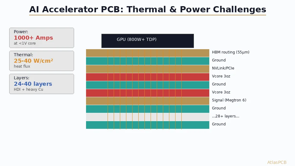
The routing density and power delivery requirements of AI servers are driving layer counts well beyond what was standard even a few years ago. Current trends:
| Platform Generation | Typical Layer Count | Trend |
|---|---|---|
| 2024 AI servers | 16-20 layers | Baseline |
| 2025-2026 platforms | 20-26 layers | Current builds |
| 2027+ roadmap | 28-34 layers | In design |
| AI networking switches | 22-30 layers | Already in volume |
This layer count escalation places enormous demands on [sequential lamination]/blog/hdi-pcb-stackup-design-advanced/) precision, registration accuracy, and drill-to-copper alignment. Each additional lamination cycle compounds manufacturing yield risks.
Power Delivery Challenges
AI GPUs are power-hungry — current-generation training chips consume 700-1000W each, and next-generation designs are pushing toward 1500W. Delivering this power through the PCB requires:
- Heavy copper inner layers (2-3 oz) for power distribution
- Extensive via arrays for vertical power delivery
- Careful [power integrity]/blog/pcb-power-integrity-decoupling/) design with embedded decoupling capacitance
- Thermal management through [thermal via arrays]/blog/pcb-thermal-via-design/)
Balancing heavy copper power layers with fine-feature signal layers in the same stackup is a manufacturing challenge that requires sophisticated [copper balancing]/blog/pcb-copper-balancing-techniques/) and registration control.
How PCB Manufacturers Are Responding
The ultra-HDI demands of AI servers are catalyzing the most significant wave of PCB manufacturing investment since the smartphone revolution drove the adoption of any-layer HDI in the early 2010s.
Capital Investment Surge
Leading PCB fabricators — particularly in Taiwan, South Korea, and Japan — have announced substantial capital expenditure programs targeting AI server PCB capabilities. Industry estimates suggest over $4 billion in cumulative PCB manufacturing investment specifically targeting ultra-HDI capabilities in 2025-2027, with the bulk focused on:
- mSAP lines: New semi-additive process production lines capable of sub-40μm trace formation
- Advanced LDI systems: [Laser direct imaging]/blog/pcb-laser-direct-imaging-ldi/) equipment with sub-10μm registration accuracy
- Precision laminators: High-accuracy vacuum lamination presses for 20+ layer any-layer builds
- Via-fill plating: Advanced copper electrofill systems for [reliable stacked microvia structures]/blog/hdi-via-reliability-thermal-cycling/)
Process Technology Evolution
The manufacturing process for AI server PCBs represents a convergence of traditional PCB fabrication and IC substrate manufacturing techniques:
Modified Semi-Additive Process (mSAP): Rather than starting with full copper foil and etching away unwanted material, mSAP begins with an ultra-thin copper seed layer (2-5μm), patterns resist, then electroplates copper only where traces are needed. This eliminates etch undercut and enables trace widths down to 30μm in production. The process requires entirely different chemistry and equipment than conventional subtractive etching.
Laser Drilling Advances: [Laser-drilled microvias]/blog/pcb-laser-drilling-microvia-technology/) for AI server boards must achieve extremely consistent hole geometries — typically 75-100μm diameter at the top with aspect ratios of 0.8:1 or better. UV laser systems are replacing CO₂ lasers for the finest features, offering cleaner hole walls and better dimensional control. Some manufacturers are implementing dual-laser systems that combine UV and CO₂ processing in a single machine.
Sequential Build-Up Reliability: Stacking microvias five or more levels deep — as required for any-layer HDI in AI server boards — creates cumulative stress during thermal cycling. Advanced [via fill and planarization]/blog/pcb-resin-plug-via-process/) techniques, combined with optimized [desmear processes]/blog/pcb-plasma-desmear-process/), are critical for ensuring long-term reliability under the harsh thermal conditions inside AI server chassis (ambient temperatures often exceeding 45°C).
The Supply Chain Impact
The concentration of ultra-HDI PCB manufacturing capability in a small number of advanced fabricators has significant supply chain implications:
Capacity Constraints
Despite the investment surge, ultra-HDI PCB capacity is expected to remain tight through at least 2028. The combination of rapidly growing AI server demand and long equipment lead times (12-18 months for key tools) means that capacity additions consistently lag demand. Lead times for [high-layer-count]/blog/high-layer-count-pcb-challenges/) AI server PCBs have stretched to 8-12 weeks, compared to 3-4 weeks for standard multilayer boards.
Cost Premium
Ultra-HDI PCBs for AI servers command significant price premiums. While a standard 12-layer FR-4 server board might cost $15-25 per unit in volume, a 24-layer ultra-HDI AI server board with mSAP processing can cost $80-200 per unit, depending on complexity. This pricing reflects both the advanced manufacturing requirements and the limited supplier base.
Geographic Concentration
Ultra-HDI PCB manufacturing capability remains heavily concentrated in East Asia:
- Taiwan: 3-4 major fabricators with production-ready mSAP capability
- South Korea: 2-3 fabricators expanding from IC substrate expertise
- Japan: 2-3 fabricators leveraging semiconductor packaging technology
- China mainland: 1-2 fabricators developing capability, with government support
This geographic concentration — and particularly the reliance on Taiwan-based manufacturers — adds supply chain risk that parallels the semiconductor industry’s own concentration challenges. Some industry observers expect this to accelerate PCB manufacturing diversification efforts, similar to the [China+1 trends]/news/global-pcb-market-southeast-asia-china-plus-one-2026/) already reshaping the broader PCB supply chain.
What This Means for the Broader PCB Industry
The AI-driven push toward ultra-HDI is having ripple effects across the entire PCB manufacturing ecosystem:
Technology Trickle-Down
Manufacturing capabilities developed for AI server PCBs inevitably migrate to other high-performance applications. Multilayer FR-4 PCB manufacturers that invest in mSAP and advanced LDI for AI applications can apply those capabilities to other demanding segments — 5G infrastructure, automotive ADAS, medical imaging, and aerospace electronics.
Workforce Development
Ultra-HDI manufacturing requires process engineers with expertise that bridges traditional PCB fabrication and semiconductor packaging. This skill set is in short supply globally, creating a talent competition that is driving up engineering salaries in the PCB manufacturing sector and accelerating training programs.
Material Innovation
The demands of AI server PCBs are driving rapid material innovation. Ultra-low-loss laminates that were once niche products are becoming mainstream requirements. Prepreg and core materials with tighter thickness tolerances, lower Dk variation, and better dimensional stability during sequential lamination are being developed specifically for this market segment.
Looking Ahead
The trajectory is clear: AI infrastructure demand will continue to push PCB technology toward capabilities that were previously the exclusive domain of IC substrates. The convergence of PCB and substrate manufacturing — sometimes called [substrate-like PCB (SLP)]/news/sam-substrate-like-pcb-technology-2026/) — is accelerating, and AI servers are the primary catalyst.
For PCB designers and procurement teams, the practical implications are:
- Engage early with capable fabricators — capacity is constrained, and building relationships now ensures access when production volumes ramp
- Design for manufacturability — work closely with your HDI PCB manufacturer during the design phase, not after layout completion
- Plan for longer lead times — ultra-HDI boards require more sequential processing steps, and capacity constraints add to cycle times
- Budget for higher costs — the advanced manufacturing required for AI server PCBs commands premium pricing that is unlikely to decrease significantly in the near term
The AI infrastructure wave is reshaping what is possible — and what is expected — in PCB manufacturing. Manufacturers that invest in these capabilities today are positioning themselves for a market that shows no signs of slowing down.
Looking for a PCB manufacturer that stays ahead of industry trends? Request a quote from Atlas PCB today.
About AtlasPCB — We specialize in complex PCB manufacturing for HDI, RF, and high-reliability applications. Explore our HDI PCB manufacturing capabilities . Every order includes free engineering review. Get your quote.
Reviewed by AtlasPCB Engineering Team — IPC-certified manufacturing specialists with 15+ years of production experience in HDI, RF, and high-reliability PCB fabrication. Content based on factory floor data and real customer design reviews.
- AI servers
- ultra-HDI
- microvia
- high layer count
- advanced manufacturing