· AtlasPCB Engineering · News · 5 min read
IBM Quantum Computing Push Creates New Requirements for PCB Supply Chain
As IBM moves quantum computers from labs to real-world installations, the electronics supply chain faces novel demands for cryogenic-compatible PCBs and ultra-low-noise interconnects.

Quantum Computing Leaves the Lab — and Needs an Electronics Supply Chain to Follow
In one of the most compelling presentations at APEX EXPO 2026, IBM’s David Lokken-Toyli, principal research scientist at IBM Quantum, described a turning point for quantum computing: the installation of a functioning quantum computer in the middle of a public cafeteria at Cleveland Clinic. As reported by iConnect007, this vivid image encapsulates a broader reality — quantum computing is transitioning from research curiosity to deployed technology, and the electronics supply chain, including PCB manufacturers, must evolve to support it.
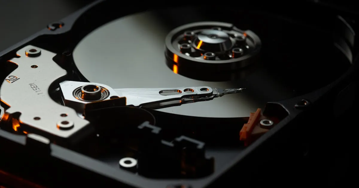
Photo by FLY:D on Unsplash — Free to use under Unsplash License
What Makes Quantum Computing PCBs Different
Traditional electronics operate at room temperature with signal frequencies typically ranging from DC to tens of GHz. Quantum computing systems operate in a fundamentally different regime, and the PCB requirements reflect this:
Cryogenic Operation
The superconducting qubits at the heart of IBM’s quantum processors operate at approximately 15 millikelvin (mK) — roughly 0.015°C above absolute zero. Reaching and maintaining this temperature requires a dilution refrigerator with multiple cooling stages:
| Stage | Temperature | Function |
|---|---|---|
| Room temperature | ~300 K | Classical control electronics |
| First stage | ~40 K | Radiation shielding, signal attenuation |
| Second stage | ~4 K | Further cooling, HEMT amplifiers |
| Still | ~800 mK | Dilution refrigerator intermediate |
| Mixing chamber | ~15 mK | Quantum processor operation |
Each temperature stage requires interconnect hardware — PCBs, flex circuits, coaxial cables, and wire bonds — that maintains functionality across enormous temperature gradients. The materials used in these interconnects must:
- Maintain mechanical integrity through thermal cycling from 300 K to 15 mK (a ΔT of nearly 300°C) without cracking, delaminating, or developing microfractures in vias or traces
- Exhibit predictable electrical behavior at cryogenic temperatures — dielectric constants and loss tangents change significantly at low temperatures for many standard PCB materials
- Minimize thermal conductivity to avoid creating heat leaks that increase the refrigerator’s thermal load and destabilize qubit operation
Standard FR-4, with its glass-epoxy composition, actually performs reasonably well at cryogenic temperatures in terms of mechanical survival. However, its dielectric properties shift enough at 4 K and below to affect carefully tuned filter and matching circuits. Materials like Rogers RT/duroid and specialized cryogenic substrates are increasingly specified for the most critical stages.
Ultra-Low Noise Requirements
Quantum bits (qubits) are extraordinarily sensitive to electromagnetic interference. A single stray photon at the qubit frequency (typically 4–8 GHz for superconducting qubits) can cause decoherence — essentially destroying the quantum information being processed. This places extreme demands on PCB design:
- Shielding: Multi-layer ground planes with comprehensive via stitching per [EMC design best practices]/blog/emc-emi-pcb-design/), but taken to levels far beyond typical commercial requirements
- Filtering: Integrated on-board filters at every signal entry point, requiring [controlled impedance]/blog/pcb-impedance-control/) structures matched to filter component characteristics
- Signal integrity: Microwave signals traveling to and from qubits must maintain phase coherence over the entire signal path. Any impedance discontinuity introduces reflections that can couple noise into qubit channels
- Grounding: Single-point grounding strategies to prevent ground loops that could introduce low-frequency magnetic noise, utilizing techniques from [advanced PCB grounding design]/blog/pcb-grounding-techniques/)
New Interconnect Architectures
The interface between the cryogenic quantum hardware and room-temperature classical control electronics represents one of the most challenging engineering problems in quantum computing. Current systems use:
- Coaxial cables: Provide excellent signal isolation but are bulky, thermally conductive, and limit system scalability. A 100-qubit system may require 200+ coaxial cables running through the cryostat
- Flex circuits: Being explored as a more compact alternative for some signal paths, leveraging [flexible PCB technology]/blog/flex-pcb-design-guidelines/) adapted for cryogenic use
- Interposer PCBs: Multi-layer boards at each temperature stage that route signals between stages while providing filtering, attenuation, and thermal isolation
As quantum computers scale from ~100 qubits (current IBM Heron processors) toward the 100,000+ qubit systems planned for the 2030s, the interconnect density must increase dramatically. This will likely require HDI-class PCBs operating at cryogenic temperatures — a combination of requirements that the PCB industry has minimal experience with today.
The Supply Chain Challenge
Lokken-Toyli’s core message was clear: getting quantum computing from the lab to the real world depends on an electronics supply chain ready to support entirely new system requirements. This creates both challenges and opportunities:
Challenges:
- Current PCB qualification standards (IPC-6012, IPC-6013) don’t address cryogenic operation
- Material characterization data at cryogenic temperatures is sparse for most PCB laminates
- Reliability testing protocols for thermal cycling between 300 K and 4 K don’t exist in standard frameworks
- Manufacturing volumes are tiny (hundreds to low thousands of boards per year), making it difficult to justify process development investments
Opportunities:
- First-mover advantage for PCB manufacturers who develop cryogenic-qualified processes
- Technology transfer potential — materials and processes developed for quantum computing may benefit other extreme-environment applications (space, superconducting power systems, particle physics detectors)
- Relationship building with quantum computing leaders (IBM, Google, Microsoft, IonQ) as they scale production
Broader Implications for High-Reliability PCB Manufacturing
Even if quantum computing remains a niche application for PCB manufacturers in the near term, the technology push is valuable. The requirements — extreme reliability, precise material characterization, novel testing protocols — align closely with capabilities already demanded by aerospace, defense, and [medical device PCB applications]/blog/medical-device-pcb-standards/).
Manufacturers who can demonstrate [IPC Class 3 high-reliability]/blog/ipc-standards-pcb-classes/) processes, comprehensive material traceability, and willingness to develop new qualification procedures are best positioned to serve the quantum computing market as it scales.
The Timeline
IBM’s quantum computing roadmap projects:
- 2026: 1,386-qubit Flamingo processor with modular architecture
- 2029: 100,000+ qubit systems with error correction
- 2030s: Quantum advantage for commercially relevant problems
Each milestone increases the number of PCBs and interconnects required per system, and raises the complexity requirements. The PCB supply chain has a window of several years to develop the materials, processes, and qualification standards needed — but that window is finite.
Atlas PCB: Ready for the Next Frontier
At Atlas PCB, our expertise in [high-reliability IPC Class 3 manufacturing]/blog/ipc-standards-pcb-classes/), [advanced materials]/blog/pcb-materials-guide/), and [complex multilayer stackups]/blog/high-layer-count-pcb-challenges/) positions us to serve emerging applications in quantum computing and other extreme-environment electronics. We’re committed to staying at the forefront of PCB technology as the industry evolves to meet these unprecedented requirements.
Working on quantum computing or extreme-environment electronics? Contact our engineering team to discuss your specialized PCB requirements, or request a quote for your high-reliability board design.
About AtlasPCB — We specialize in complex PCB manufacturing for HDI, RF, and high-reliability applications. Explore our full PCB manufacturing capabilities, or get an instant online quote . Every order includes free engineering review. Get your quote.
Reviewed by AtlasPCB Engineering Team — IPC-certified manufacturing specialists with 15+ years of production experience in HDI, RF, and high-reliability PCB fabrication. Content based on factory floor data and real customer design reviews.
- news
- quantum-computing
- electronics-supply-chain
- advanced-manufacturing
- ibm