· AtlasPCB Engineering · News · 3 min read
AI and ML Hardware Driving Unprecedented Demand for High-Layer-Count PCBs
The explosive growth of AI/ML training and inference hardware is pushing PCB layer counts to new extremes, with 40-68 layer boards becoming standard for next-generation GPU and ASIC platforms.
The artificial intelligence revolution is transforming the PCB industry in ways few predicted even two years ago. As AI training clusters scale from thousands to hundreds of thousands of GPUs, and inference deployments push into edge computing, the demand for ultra-high layer count PCBs has surged to unprecedented levels.
The Layer Count Arms Race
Modern AI accelerator platforms—including NVIDIA’s Blackwell B200/B300 series, AMD’s Instinct MI400, and a growing roster of custom ASICs from hyperscalers like Google (TPU v6), Amazon (Trainium 3), and Microsoft (Maia 2)—are driving board complexity to new heights.
These platforms share several characteristics that demand high layer counts:
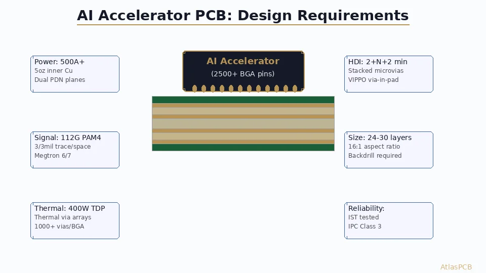
- Massive I/O density: A single next-gen GPU package can have 5,000–7,000+ signal pins, each requiring controlled-impedance routing through the package breakout zone
- High-speed serial links: PCIe Gen 6 (64 GT/s PAM4), NVLink, CXL 3.0, and 800G Ethernet connections each require dedicated stripline routing layers with adjacent ground reference planes
- Power delivery: AI accelerators consuming 700–1000W per chip require multiple power domains with heavy copper planes and extensive decoupling networks
- Signal integrity: Maintaining signal quality at 56–112 Gbps per lane demands careful stackup design with low-loss materials and back-drilled vias
The result: server boards for AI clusters now routinely specify 36–48 layers, with leading-edge designs reaching 56–68 layers. This represents a significant increase from the 24–32 layer standard of just three years ago.
Manufacturing Challenges
This demand surge creates significant manufacturing challenges. As detailed in our [high layer count PCB challenges guide]/blog/high-layer-count-pcb-challenges/), boards above 40 layers require:
- Advanced registration systems (X-ray alignment with ±25µm tolerance)
- Pulse-reverse plating for high aspect ratio through-holes (15:1–20:1)
- Premium materials (Megtron 6/7, Isola I-Speed) for low-loss signal transmission
- Back-drilling with ±0.1mm accuracy for stub elimination on high-speed vias
The yield challenge is particularly acute. With 50+ inner layers, even a 1% per-layer defect rate compounds to significant scrap. Fabricators are investing heavily in LDI (Laser Direct Imaging) for improved inner layer accuracy and AI-powered AOI systems for defect detection.
Supply Chain Implications
The AI hardware boom has tightened the supply chain for high-layer-count PCBs:
- Lead times for 40+ layer boards have extended from 15–20 days to 25–35 days at many fabricators
- Material availability for specialty laminates (particularly low-loss, low-CTE materials) has become constrained
- Capacity allocation at fabricators qualified for 50+ layer production is increasingly committed to hyperscaler contracts months in advance
Market Projections
Industry analysts project the AI-driven high-layer-count PCB market will grow at a 25–30% CAGR through 2028, compared to 5–7% for the overall PCB market. The key growth drivers:
- Training cluster expansion: Major hyperscalers are building 100,000+ GPU clusters, each requiring thousands of high-layer-count server boards
- Inference deployment: As AI inference moves to edge locations, high-performance PCBs are needed at scale beyond data centers
- Networking infrastructure: 800G and 1.6T switch platforms supporting AI clusters require 40+ layer switch boards
- Memory subsystems: HBM (High Bandwidth Memory) interposer substrates and associated PCBs are adding to demand
Atlas PCB’s Position
At Atlas PCB, we have expanded our high-layer-count manufacturing capacity to meet this growing demand. Our capabilities include:
- Manufacturing up to 68 layers with IPC-6012 Class 3 certification
- Advanced materials including Megtron 6, I-Speed, and hybrid stackups
- Pulse-reverse plating for aspect ratios up to 20:1
- Back-drilling with ±0.1mm depth control
- Dedicated production lines for AI/data center boards with prioritized scheduling
For AI hardware designers facing tight timelines and demanding specifications, we offer engineering consultation on stackup optimization and DFM review. Contact us for a quote on your next AI platform design.
The convergence of AI demand with advancing PCB technology is creating one of the most dynamic periods in PCB manufacturing history. Designers and fabricators who can navigate the complexity of 40–68 layer boards while maintaining quality and delivery schedules will be well-positioned for the AI era.
About AtlasPCB — We specialize in complex PCB manufacturing for HDI, RF, and high-reliability applications. Explore our full PCB manufacturing capabilities, or get an instant online quote . Every order includes free engineering review. Get your quote.
Reviewed by AtlasPCB Engineering Team — IPC-certified manufacturing specialists with 15+ years of production experience in HDI, RF, and high-reliability PCB fabrication. Content based on factory floor data and real customer design reviews.
- news
- AI hardware
- high layer count
- data center
- GPU