· AtlasPCB Engineering · Engineering · 14 min read
1oz vs 2oz Copper PCB: When to Upgrade Copper Weight and What It Costs
A manufacturer's comparison of 1oz and 2oz copper PCB construction covering current carrying capacity, trace width implications, impedance control adjustments, manufacturing yield impact, and real cost differences. Includes a decision matrix with concrete current thresholds for choosing the right copper weight.

Quick Answer
Choose 2oz copper when any trace on your board must carry more than 1A continuously in external layers or more than 0.5A in internal layers at the minimum trace width your design rules permit. For a standard 10mil (0.25mm) trace, 1oz copper handles approximately 1.0A with a 10C temperature rise while 2oz handles approximately 1.5A — a 50% increase in current capacity for approximately 15-25% additional board cost. The primary manufacturing trade-off is that 2oz copper requires wider minimum trace and space rules (typically 5/5mil vs 4/4mil for 1oz) due to the increased etch factor.
Quick Answer: When 2oz Copper Pays for Itself
The decision between 1oz and 2oz copper comes down to a single question: does any trace on your board need to carry more current than your minimum trace width can handle at 1oz thickness? If you are routing power rails at currents above 1A on 10mil traces, or if thermal dissipation from copper spreading is critical to your design (LED drivers, motor controllers, power converters), then 2oz copper on at least the outer layers is almost certainly the right choice. If your board is purely signal routing with power delivery handled through planes and wide polygon pours, 1oz copper handles the job at lower cost and with finer routing capability.
The practical threshold from our production experience: boards where the highest-current trace carries less than 0.75A at the designer’s minimum trace width work well at 1oz. Boards with power traces carrying 1-3A benefit from 2oz outer copper. Boards exceeding 3A per trace should consider 3oz or dedicated heavy copper construction.
| Parameter | 1oz Copper (35um) | 2oz Copper (70um) | Impact |
|---|---|---|---|
| Current capacity (10mil trace, 10C rise) | ~1.0A external | ~1.5A external | +50% |
| Minimum trace width | 3.5-4.0mil | 5.0mil | Wider at 2oz |
| Minimum space | 3.5-4.0mil | 5.0mil | Wider at 2oz |
| 50-ohm microstrip width (4mil to GND) | ~4.2mil | ~5.8mil | 40% wider |
| Cost premium (outer layers only) | Baseline | +10-15% | Moderate |
| Cost premium (all layers 2oz) | Baseline | +15-25% | Significant |
| Etch factor (lateral:vertical) | ~2.5:1 | ~3:1 | More undercut |
| Typical applications | Signal routing, digital logic | Power delivery, LED, motor drive | — |
Need help choosing copper weight for your design?
Upload your design files and our engineers will analyze your power traces, calculate required copper weight for your current requirements, and recommend the most cost-effective stackup configuration. Free with every quote request.
Get a Free Copper Weight RecommendationCurrent Carrying Capacity: The Real Numbers
The relationship between copper weight and current capacity follows IPC-2152, which replaced the older IPC-2221 charts that significantly underestimated current capacity for modern PCB constructions. The critical insight is that current capacity depends on the cross-sectional area of the conductor (width multiplied by thickness), the acceptable temperature rise above ambient, and whether the trace is on an external layer (better heat dissipation to air) or buried internally (heat trapped between dielectric layers).
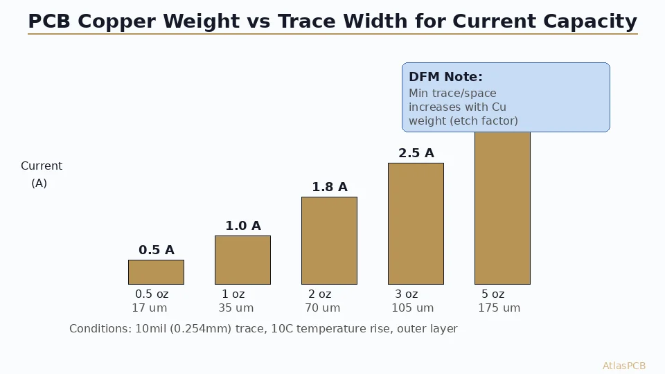
For external layers (microstrip traces exposed to air on one side), the temperature rise for a given current scales inversely with conductor cross-section. Doubling the copper thickness from 1oz (35um) to 2oz (70um) doubles the cross-sectional area for the same trace width, but current capacity does not simply double because heat dissipation also changes. In practice, 2oz copper provides approximately 40-50% more current capacity than 1oz for the same trace width and temperature rise.
The following table provides current capacity values calculated from IPC-2152 for common trace widths at both copper weights, assuming a 10 degrees Celsius temperature rise above ambient on external layers:
| Trace Width | 1oz External | 2oz External | 1oz Internal | 2oz Internal |
|---|---|---|---|---|
| 5mil (0.127mm) | 0.6A | 0.9A | 0.4A | 0.6A |
| 10mil (0.254mm) | 1.0A | 1.5A | 0.7A | 1.0A |
| 15mil (0.381mm) | 1.4A | 2.0A | 0.9A | 1.4A |
| 20mil (0.508mm) | 1.7A | 2.5A | 1.2A | 1.7A |
| 30mil (0.762mm) | 2.3A | 3.3A | 1.6A | 2.3A |
| 50mil (1.27mm) | 3.2A | 4.6A | 2.2A | 3.2A |
| 100mil (2.54mm) | 5.2A | 7.5A | 3.6A | 5.2A |
Internal layers carry significantly less current than external layers at the same trace width and copper weight because they cannot dissipate heat to the surrounding air. The dielectric material surrounding internal traces has poor thermal conductivity (approximately 0.3 W/m-K for FR-4 compared to 25 W/m-K for air convection equivalent), so heat must conduct laterally through copper to reach the board edges or vertically through vias to external copper planes for dissipation.
A subtle but important point: the temperature rise values assume the trace operates in isolation. In real designs with closely spaced parallel traces all carrying current, the mutual heating effect raises the baseline temperature of the surrounding copper, reducing the effective current capacity by 10-20% compared to isolated-trace calculations. When multiple power traces route in parallel on the same layer, apply a 15% derating to the values above.
Manufacturing Impact: What Changes at 2oz Copper
From a fabrication perspective, the difference between 1oz and 2oz copper is not trivial. Every process step that interacts with the copper layer is affected, and understanding these manufacturing realities explains both the cost premium and the design rule restrictions that 2oz copper imposes.
The etch process represents the most significant manufacturing change. Standard 1oz copper (35um thick) etches in approximately 90 seconds using alkaline ammoniacal etchant at standard concentration and temperature. During that time, lateral etching (undercutting beneath the photoresist) proceeds at a rate of roughly one-third to one-half the vertical etch rate, removing approximately 10-15um from each side of the trace. This lateral etch is called the etch factor, expressed as the ratio of vertical etch depth to lateral etch per side. For 1oz copper, a typical etch factor is 2.5:1 to 3:1.
At 2oz copper (70um thick), the etch time approximately doubles because the etchant must dissolve twice the copper depth. But lateral etching also continues for that doubled time, removing approximately 20-25um from each side. This means that a trace designed at 5mil (127um) nominal width on the photomask will finish at approximately 4-4.5mil (100-115um) after 2oz etching. To compensate, the manufacturer applies etch compensation, widening the trace image on the photomask so that the final etched trace matches the design intent. This compensation is automated in our CAM systems, but it requires the designer to leave sufficient space between traces to accommodate the wider mask artwork.
The practical consequence is straightforward: minimum achievable trace width and spacing increases with copper weight. At 1oz, our process reliably produces 3.5/3.5mil (89/89um) trace and space on inner layers and 3.5/3.5mil on outer layers for standard panel sizes. At 2oz, these minimums increase to 5/5mil (127/127um) on both inner and outer layers. Attempting finer geometry at 2oz copper results in over-etching that narrows traces below specification or creates open circuits, reducing yield below economically viable levels.
Inner-layer processing is particularly affected because inner layers undergo both imaging and etching before lamination. At 2oz inner copper, the etching step produces more aggressive undercut, but more importantly, the thicker copper creates greater surface topography that the prepreg must fill during lamination. If copper coverage on a 2oz inner layer is uneven (dense routing in one area, sparse in another), the prepreg may not fully planarize the surface, creating voids or thickness variation that affects impedance control and long-term reliability.
Impedance Control with 2oz Copper
Copper thickness directly affects characteristic impedance because it changes the cross-sectional geometry of the transmission line structure. For microstrip (an external trace referenced to a ground plane below), impedance depends on trace width, trace thickness, dielectric height, and dielectric constant. When copper thickness doubles from 1oz to 2oz, the trace cross-section becomes taller, which increases capacitance to the reference plane and decreases impedance for the same trace width.
To maintain the same target impedance at 2oz copper, the trace must be made wider to compensate for the increased thickness. The magnitude of this adjustment depends on the specific geometry, but as a representative example: for a microstrip trace on an outer layer with 4mil (100um) dielectric spacing to the adjacent ground plane and Dk of 4.2, a 50-ohm impedance target requires approximately 4.2mil trace width at 1oz (35um copper) but approximately 5.8mil at 2oz (70um copper). This 40% increase in trace width has cascading effects on routing density, especially for impedance-controlled differential pairs where both the trace width and the pair-to-pair spacing must increase proportionally.
For impedance-controlled designs, the stackup document must specify copper weight per layer so that the impedance modeling accurately predicts the required trace geometry. A common mistake we see is designers who specify 2oz outer copper for current capacity on power traces but forget that their impedance-controlled signal traces on the same layer will require recalculated widths. The impedance modeling must use the actual copper weight that will be present after plating. On outer layers, the final copper thickness is the base foil plus approximately 20-25um of electroplated copper added during the panel plating step, so a 1oz base foil becomes approximately 55um final thickness and a 2oz base foil becomes approximately 90-95um.
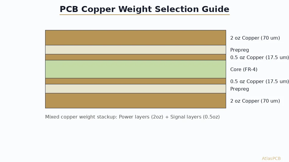
This is why the most common approach for designs requiring both fine-pitch impedance-controlled routing and high-current power delivery is to use mixed copper weights: 1oz or 0.5oz on inner signal layers where trace width must remain tight for impedance control, and 2oz on outer layers where power traces need the extra current capacity and where the wider impedance-controlled traces still fit within the available routing space.
Mixed copper weight stackup — designed for your specs
Our engineers will model impedance for your specific copper weights and dielectric materials, delivering trace width calculations that account for plating buildup, etch compensation, and your current capacity requirements. No guesswork needed.
Get Impedance Modeling for Your StackupThermal Performance and IR Drop
Beyond current capacity, copper weight affects two thermal parameters that matter for power electronics and high-reliability designs: lateral heat spreading and voltage drop (IR drop) across the board.
Thermal spreading refers to the ability of copper planes and wide traces to conduct heat laterally from a hot spot (such as a power MOSFET or voltage regulator) toward a larger area where it can dissipate to the environment. Copper’s thermal conductivity is approximately 390 W/m-K, vastly superior to the FR-4 dielectric below it (0.3 W/m-K). A 2oz copper plane spreads heat from a point source approximately 40% more effectively than a 1oz plane of the same area because the thicker copper provides more cross-sectional area for lateral conduction. This translates directly to lower component junction temperatures in designs where the PCB itself serves as the primary heat sink.
IR drop — the voltage lost across a copper trace due to its DC resistance — scales inversely with copper cross-section. For a trace carrying current I with resistance R, the voltage drop equals I multiplied by R, where R equals resistivity multiplied by length divided by cross-sectional area. Doubling the copper thickness halves the resistance (and therefore halves the IR drop) for the same trace geometry. In power distribution networks for FPGAs and processors requiring tight voltage regulation (plus or minus 3% of nominal), reducing IR drop through thicker copper can be the difference between meeting the voltage margin at the die pad and violating it.
As a practical example: a 2-inch (50mm) power trace at 20mil width carrying 2A has a DC resistance of approximately 45 milliohms at 1oz copper and approximately 22 milliohms at 2oz. The resulting voltage drops are 90mV and 44mV respectively. For a 1.0V core rail, the 1oz trace consumes 9% of the voltage budget in IR drop alone, while the 2oz trace consumes only 4.4%. This margin improvement often justifies the cost premium of 2oz copper in processor power delivery applications.
Cost Analysis: Real Pricing Differences
The cost impact of upgrading copper weight varies by which layers are affected and by production volume. Our current pricing structure reflects the following incremental costs for a representative board (100mm x 100mm, 6 layers, ENIG, standard FR-4 Tg170):
| Configuration | Prototype (10 pcs) | Production (1000 pcs) | Premium vs All-1oz |
|---|---|---|---|
| All layers 1oz | $28-35/board | $3.50-5.00/board | Baseline |
| Outer 2oz / Inner 1oz | $32-40/board | $4.00-5.50/board | +12-15% |
| Outer 2oz / Inner 2oz | $35-45/board | $4.50-6.50/board | +20-30% |
| Outer 3oz / Inner 1oz | $42-55/board | $5.50-7.50/board | +45-60% |
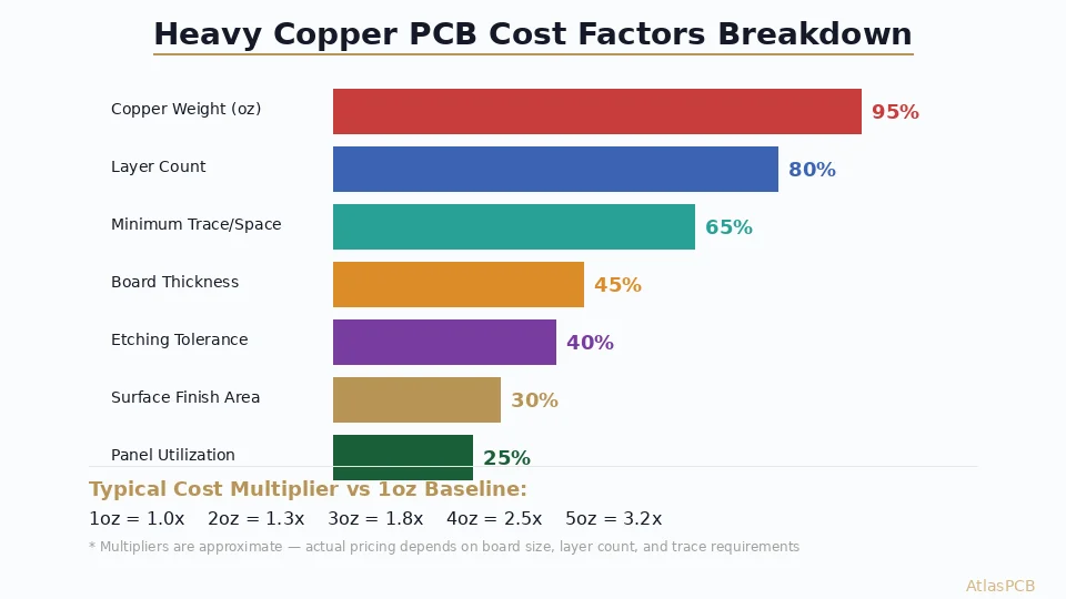
The cost drivers at 2oz are: additional copper foil material cost (minimal, approximately 5% of total), increased etching time reducing throughput on the etch line, additional etch compensation engineering in CAM, and reduced first-pass yield (approximately 2-3% lower yield at 2oz inner copper compared to 1oz at equivalent design rules).
At production volumes, the material cost differential becomes a smaller fraction of total cost, so the percentage premium decreases. However, the yield impact remains constant regardless of volume, which is why even at high volumes the 2oz premium never fully disappears.
Decision Matrix: 1oz vs 2oz vs 3oz
The following matrix provides concrete guidance for selecting copper weight based on design requirements:
| Application | Max Current per Trace | Recommended Copper | Min Trace/Space | Notes |
|---|---|---|---|---|
| Digital logic (MCU, FPGA) | Under 0.5A | 1oz outer, 0.5oz inner | 3.5/3.5mil | Fine routing, impedance-controlled |
| Mixed signal (ADC, DAC) | Under 0.5A | 1oz all layers | 4/4mil | Uniform copper for consistent impedance |
| LED driver | 0.5-2A | 2oz outer, 1oz inner | 5/5mil outer | 2oz on LED power rails |
| Motor driver (BLDC) | 1-5A | 2oz outer, 1oz inner | 5/5mil outer | Consider thermal vias under MOSFETs |
| Power converter (DC-DC) | 2-10A | 2oz-3oz outer, 1oz inner | 6/6mil | May need heavy copper above 5A |
| Automotive power distribution | 3-15A | 3oz-5oz outer, 2oz inner | 8/8mil | IPC Class 3, heavy copper |
| Server/networking (high-speed) | Under 0.5A signals, 1-3A power | 1oz outer, 0.5oz inner | 3.5/3.5mil | Impedance priority over current |
| RF/microwave | Minimal | 0.5oz or 1oz | 3/3mil | Thinner copper = tighter impedance |
The critical rule: never let power delivery requirements force your signal traces to be wider than optimal for impedance control. If you need both high current AND fine-pitch signal routing on the same board, use mixed copper weights (heavy on power layers, light on signal layers) rather than forcing a single copper weight to serve both purposes.
Designing a power-dense PCB?
Our engineers specialize in mixed copper weight designs that deliver maximum current capacity without compromising signal integrity. From 0.5oz inner layers for controlled impedance to 5oz outer layers for bus bars, we manufacture the full range. Tell us your current requirements and we will recommend the optimal copper configuration.
Get a Power PCB QuoteDFM Guidelines for 2oz Copper Designs
When designing a board with 2oz copper on any layer, the following manufacturing constraints must be reflected in your design rules to ensure reliable fabrication and acceptable yield:
Minimum trace width must increase to 5mil (127um) on 2oz layers. Specifying 4mil traces at 2oz is technically possible on some advanced production lines but reduces yield significantly and should only be attempted after discussing feasibility with your manufacturer. The wider minimum exists because the etch compensation required at 2oz (approximately 0.8-1.0mil added per side on the phototool) leaves less margin for process variation before traces become open circuits or shorts.
Minimum spacing between traces must also increase to 5mil at 2oz. The lateral etch profile at 2oz creates a trapezoidal cross-section where the trace is wider at the base (attached to the dielectric) than at the top (where etching initiated). If designed spacing is too tight, the bases of adjacent traces may approach each other even when tops appear adequately separated, creating a reliability risk under voltage stress and humidity exposure.
Annular ring requirements increase for via pads on 2oz copper layers. The standard minimum annular ring of 3.5mil at 1oz should increase to 4.5-5mil at 2oz because the thicker copper requires more aggressive etching around the pad perimeter, and registration tolerance between the drill and the pad artwork compounds with the etch undercut to reduce the effective annular ring.
Solder mask registration becomes more demanding on 2oz outer layers. The thicker copper creates more pronounced surface topography that the solder mask must bridge across trace edges. Solder mask dams (the mask material between adjacent pads) should be minimum 4mil at 2oz, compared to 3mil at 1oz. Narrower dams risk cracking or bridging over the steep copper edges.
Copper balance across layers remains important but becomes more critical at 2oz. The thicker copper generates more internal stress during thermal cycling, and asymmetric copper distribution exacerbates warpage. Ensure copper coverage varies by no more than 20% between any two layers, adding thieving patterns where necessary.
For boards requiring both fine-pitch signal routing and 2oz power distribution, the recommended approach is to separate these functions onto different layers: use 0.5oz or 1oz copper on inner signal layers where 3.5-4mil trace width and spacing are needed for BGA escape routing and impedance control, and place 2oz copper only on the outer layers and dedicated power plane layers where the wider design rules are acceptable.
Reviewed by AtlasPCB Engineering Team — 15+ years in advanced PCB fabrication for RF, HDI, and rigid-flex applications.
Related Reading:
About AtlasPCB — We specialize in complex PCB manufacturing for HDI, RF, and high-reliability applications. Explore our heavy copper PCB manufacturing, free engineering DFM review, or get an full PCB manufacturing capabilities . Every order includes free engineering review. Get your quote.
Reviewed by AtlasPCB Engineering Team — IPC-certified manufacturing specialists with 15+ years of production experience in HDI, RF, and high-reliability PCB fabrication. Content based on factory floor data and real customer design reviews.
Frequently Asked Questions
How much more current can 2oz copper carry than 1oz?
How much does 2oz copper add to PCB cost?
What is the minimum trace width for 2oz copper?
Does 2oz copper affect impedance?
Can I mix 1oz and 2oz copper in the same PCB?
- copper weight
- PCB design
- 1oz copper
- 2oz copper
- current capacity
- PCB manufacturing
- DFM
- heavy copper
- power PCB