· AtlasPCB Engineering · Engineering · 13 min read
How to Specify Impedance Control in Your PCB Fab Drawing: The Complete DFM Guide
Step-by-step guide for specifying impedance control requirements in PCB fabrication drawings. Covers impedance tables, tolerance selection, reference plane definition, Dk documentation, measurement standards, and the common DFM mistakes that cause impedance failures. Written for hardware engineers preparing to order their first impedance-controlled board.
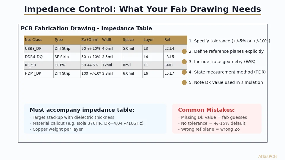
Quick Answer
To specify impedance control correctly, your PCB fab drawing must include: (1) an impedance table listing every controlled net class with target Zo, tolerance, trace width/space, layer assignment, and reference planes; (2) the target stackup with specific dielectric thicknesses and material Dk values at your operating frequency; (3) the measurement standard (IPC-TM-650 2.5.5.7 TDR method); and (4) a note stating whether the manufacturer may adjust trace width to meet impedance targets. Missing any of these forces the fab to guess — and guesses cause impedance failures.
Quick Answer: The 5 Things Your Fab Drawing Must Include
Every impedance-controlled PCB fabrication drawing needs these elements. Missing any single one forces the manufacturer to make assumptions that may not match your simulation:
- Impedance Table — Net class, target Zo (ohms), tolerance (+/-%), trace width, spacing (differential), signal layer, reference plane(s)
- Target Stackup — Layer-by-layer dielectric thickness, copper weight, material specification
- Dk Value with Frequency — The dielectric constant you used in simulation, at what frequency
- Measurement Standard — “Per IPC-TM-650 2.5.5.7” (TDR method on coupon)
- Width Adjustment Permission — Whether the fab may modify trace width to achieve impedance
If your fab drawing has all five, you will get boards that match your simulation. If it’s missing even one, you’re rolling dice.
Why Impedance Control Fails: The DFM Gap
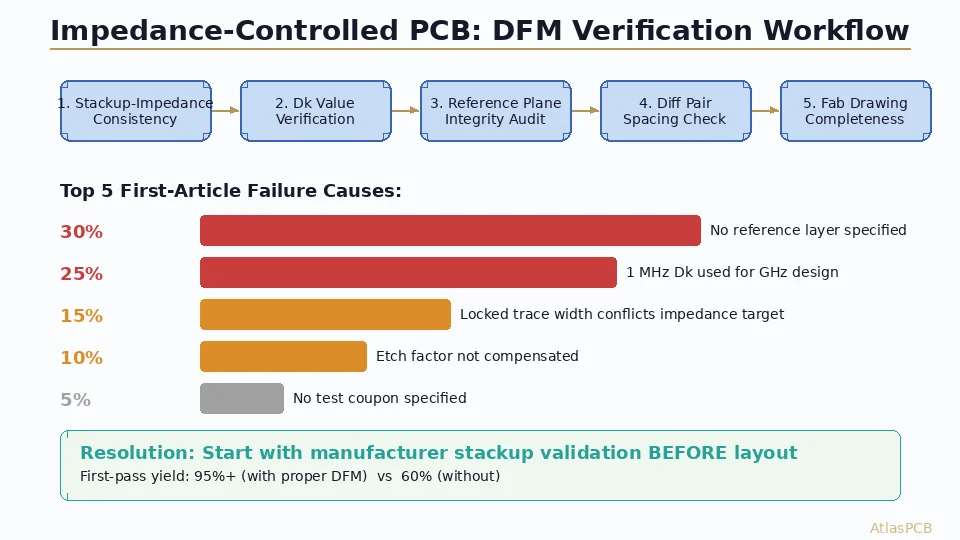
The most common cause of impedance failure is not manufacturing error — it’s incomplete specification. In our facility, we review approximately 400 impedance-controlled designs per month. Of those, roughly 30% arrive with specifications that cannot be fabricated as drawn without clarification. The engineer’s simulation was correct, but the information transferred to the manufacturer was incomplete.
The root issue is that impedance is not a single parameter — it’s an emergent property of trace geometry, dielectric thickness, dielectric constant, copper roughness, and solder mask thickness. Your simulation tool (Polar Si9000, Altium’s impedance calculator, Ansys HFSS) accounts for all these variables internally. But when you write “50 ohm +/-10%” on your fab drawing without specifying which variables you assumed, the manufacturer must reverse-engineer your intent.
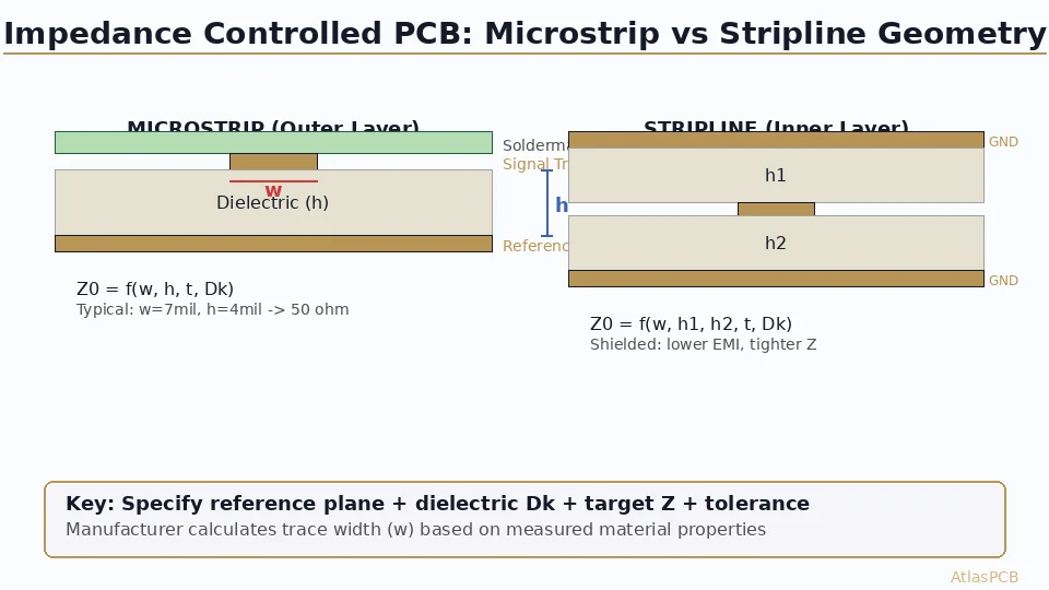
Consider a 50-ohm microstrip on Layer 1 of a 6-layer board. The impedance depends on: trace width (your design), dielectric height to the reference plane (your stackup), Dk of the prepreg (material-specific), copper roughness (process-specific), and solder mask effect (adds 2-5% to effective Dk). If your simulation assumed Dk = 4.2 for generic FR-4 but the manufacturer uses Isola 370HR (Dk = 4.04 at your frequency), the impedance will be 3-4 ohms higher than your target — potentially outside the +/-10% tolerance window before any manufacturing variation is even considered.
This is why our DFM engineers always ask for the complete stackup with material callout before starting impedance-controlled production. It’s not bureaucracy — it’s the only way to ensure the boards you receive match the boards you simulated.
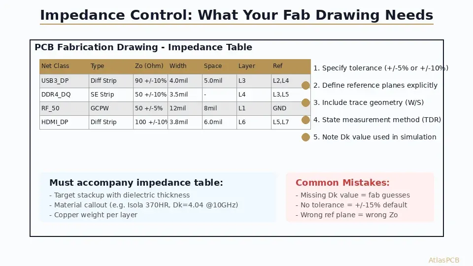
IMPEDANCE CONTROLLED PCB
Free DFM Review for Impedance-Controlled Boards
Upload your Gerber + stackup. Our engineers verify impedance feasibility, check reference plane continuity, and confirm Dk assumptions before production starts.
Upload Design Files ›
Building the Impedance Table: Field by Field
Your impedance table is the single most important element of the fab drawing for controlled-impedance boards. Here’s what each column must contain and why:
Net Class / Signal Group: Group signals by impedance requirement, not by individual net name. “USB3_DP” is better than listing all 47 individual USB differential pairs. The manufacturer needs to know which traces on which layers require control — not every net name in your schematic.
Impedance Type: Explicitly state whether each entry is single-ended (microstrip or stripline), differential (edge-coupled microstrip or broadside-coupled stripline), or coplanar (GCPW, CPW). Never assume the manufacturer will figure this out from context. We’ve seen differential pairs specified as “100 ohm” where the engineer meant 100 ohm differential (50 ohm per line) but the fab interpreted it as 100 ohm single-ended — resulting in traces too narrow to manufacture.
Target Impedance: State the target in ohms with the tolerance. For differential pairs, state BOTH the single-ended and differential target: “Zdiff = 90 ohm (Zse = 45 ohm per line), +/-10%.” This eliminates any ambiguity about whether you’re specifying odd-mode or differential impedance.
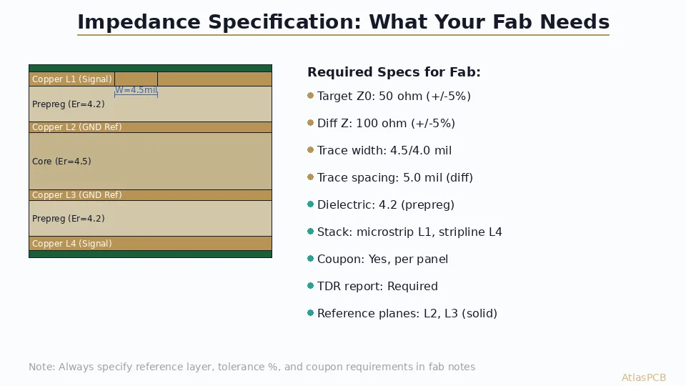
Trace Width / Spacing: Include the trace width and pair spacing from your simulation as the starting geometry. These are the values the manufacturer uses as a baseline before running their own impedance simulation with actual material data. A typical entry: “W = 4.0 mil, S = 5.5 mil (from Polar Si9000, Dk = 4.04).”
Signal Layer: State which layer(s) this impedance requirement applies to. Different layers have different dielectric thicknesses and reference plane configurations, so “50 ohm” on Layer 3 requires a different trace width than “50 ohm” on Layer 1.
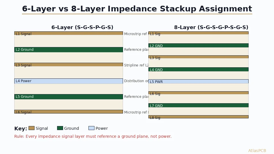
Reference Plane(s): For microstrip (outer layers), state the immediate reference ground plane: “L1 referenced to L2 (GND).” For stripline (inner layers), state BOTH reference planes: “L4 referenced to L3 (GND) and L5 (GND).” If either reference plane has splits, voids, or is a power plane rather than a continuous ground, note this explicitly — the manufacturer cannot see your power plane shapes from the impedance table alone.
Stackup Specification: What the Fab Actually Needs
The impedance table tells the manufacturer WHAT to achieve. The target stackup tells them HOW to build it. These must be consistent with each other, and both must be present.
A proper stackup specification for impedance-controlled boards includes:
Layer-by-layer construction: State every layer from top to bottom — copper layers, prepreg layers, core layers — with their nominal thickness. For impedance-critical dielectrics, state the thickness to 0.1 mil resolution: “Prepreg L1-L2: 4.0 mil (1x 1080 glass style, 65% resin content).” The glass style and resin content matter because they determine the actual Dk — the same prepreg designation can have different Dk values depending on resin percentage.
Material specification: Name the specific laminate system. “FR-4” is not a specification — it’s a material family with Dk ranging from 3.8 to 4.8 depending on manufacturer and glass style. Acceptable callouts: “Isola 370HR,” “Shengyi S1000-2M,” “Panasonic Megtron 6.” If cost is a concern, state “Isola 370HR or equivalent (Dk = 4.04 +/-0.05 at 10 GHz)” to allow material substitution.
Dk value at frequency: This is the field most engineers omit — and it’s the one that causes the most impedance failures. State the Dk value you used in your impedance simulation AND the frequency at which it applies. Example: “Dk = 4.04 at 10 GHz (per Isola 370HR Dk/Df datasheet, measurement method IPC-TM-650 2.5.5.5, clamped stripline).” This single line eliminates the most common source of systematic impedance error.
Copper weight per layer: State the finished copper weight (after plating for outer layers). Outer layers with 1 oz base copper will be approximately 1.7 oz after panel plating and pattern plating. This thicker copper slightly reduces the effective dielectric height — a correction of 0.3-0.5 mil that matters for tight-tolerance designs.
In our process, when a customer provides a complete stackup with Dk callout, we achieve first-pass impedance yield above 95% (meaning 95% of coupon measurements fall within the specified tolerance on the first production run). When the Dk is not specified and we must assume our process default, first-pass yield drops to approximately 82% — necessitating trace width iteration on the second panel, which adds 2-3 days to the schedule.
PCB DFM CHECK
Stackup Optimization Before Production
Our engineers simulate your impedance targets against our actual material inventory and process data. We confirm feasibility or suggest optimizations before panel fabrication starts.
Submit Stackup for Review ›The 7 Most Common Impedance Specification Mistakes
Based on approximately 4,800 impedance-controlled designs we’ve processed in the past year, these are the errors our DFM team catches most frequently — ranked by occurrence:
1. No Dk value specified (38% of designs). The engineer simulated with Polar’s default “generic FR-4” Dk of 4.2, but the actual material (Isola 370HR) has Dk = 4.04 at their operating frequency. Result: 3-5% systematic impedance offset that pushes tight-tolerance designs out of spec.
2. Reference plane not explicitly stated (24% of designs). For inner-layer stripline, the engineer assumed both adjacent layers are solid ground. But Layer 5 in their design is actually a split power plane with a 40-mil gap under a signal trace group. The impedance in that region is 8-12% higher than the target because the reference plane is effectively absent on one side.
3. Differential impedance stated without single-ended target (18% of designs). “100 ohm differential” can mean different things depending on coupling. If the pair is loosely coupled (space > 3x width), Zdiff is approximately 2x Zse and each line is approximately 50 ohm. If tightly coupled (space = width), each line might be 60 ohm with Zdiff = 100 ohm due to odd-mode coupling. The manufacturer needs both values to verify.
4. Missing width adjustment note (15% of designs). The engineer drew traces at exactly 4.0 mil based on simulation. But the actual prepreg thickness is 4.2 mil (within laminate tolerance), making the impedance 2 ohms high. If the fab has permission to adjust to 4.3 mil trace width, they hit the target. Without permission, they must either ship out-of-spec boards or call for a deviation — adding 1-2 days.
5. Solder mask effect ignored (12% of designs). Solder mask adds 2-3 mil of dielectric material over outer-layer microstrip traces, lowering impedance by 2-5% depending on mask thickness and Dk. If your simulation doesn’t include solder mask (many don’t by default), your 50 ohm microstrip will measure 48-49 ohm at the manufacturer. For +/-10% tolerance this is fine; for +/-5% it can be the difference between pass and fail.
6. Mixed tolerance on a single layer (8% of designs). “USB3 = 90 ohm +/-10%, PCIe Gen5 = 85 ohm +/-5%” on the same layer creates a manufacturing conflict. The trace width adjustment needed for the +/-5% net may affect the +/-10% net through etch compensation changes. We recommend keeping all nets on a given layer at the same tolerance tier, or physically separating them by region.
7. Impedance called out on non-length-matched pairs (5% of designs). The impedance table shows controlled differential pairs, but the design has no length matching within pairs — some pairs have 200+ mil intra-pair skew. Impedance control is pointless without matching: a 200 mil skew on a 90 ohm pair creates a common-mode conversion that no amount of impedance accuracy can compensate.
Tolerance Selection: Matching Cost to Requirement
Impedance tolerance directly drives board cost because tighter tolerance means tighter process control, more frequent coupon testing, higher scrap rates, and potentially restricted material choices. Here’s what each tolerance tier actually costs and requires:
+/-10% (standard): No cost premium. Achievable by any competent multilayer manufacturer using standard process controls. First-pass panel yield above 95%. Appropriate for: USB 2.0/3.0, DDR3/DDR4, HDMI 1.4/2.0, PCIe Gen 1-4, standard LVDS, 1G/10G Ethernet.
+/-7% (enhanced): Adds 5-10% to board cost. Requires tighter prepreg thickness control (selecting specific lot codes), more coupon measurement points, and potentially trace width pre-compensation based on material incoming inspection data. First-pass yield approximately 90%. Appropriate for: PCIe Gen 5/6, 25G+ SerDes, DDR5, HDMI 2.1, USB4.
+/-5% (precision): Adds 15-25% to board cost. Requires incoming material Dk verification, lot-specific impedance simulation, potentially iterative trace width adjustment (first panel as test run), and 100% coupon testing on every panel. First-pass yield approximately 80%. Appropriate for: 56G PAM4, 112G SerDes, mmWave RF, automotive radar, high-reliability defense.
+/-3% (ultra-precision): Adds 40-60% to board cost. Requires dedicated material lots, individual panel impedance tuning, multiple coupon test points per panel, and potentially controlled ambient conditions during imaging. First-pass yield approximately 65%. Only a handful of manufacturers worldwide can reliably achieve this. Appropriate for: metrology-grade RF, calibration standards, satellite transponder filters.
The engineering decision is: what tolerance does your link budget actually need? If your signal integrity simulation shows 3 dB of margin at 10% impedance variation, specifying 5% tolerance wastes money. We see this frequently — engineers specify +/-5% “to be safe” when their actual margin analysis shows +/-10% is fine, adding 20% to board cost with no functional benefit.
IMPEDANCE CONTROLLED PCB MANUFACTURER
Impedance Control from +/-10% to +/-5%
We provide TDR measurement reports with every impedance-controlled order. Up to 30 layers, all materials (FR-4, Rogers, Megtron), with coupon data traceable to your specific panels.
Compare Prices ›Measurement and Verification: What to Expect from Your Manufacturer
When you specify impedance control, the manufacturer adds test coupons to the production panel — small trace structures that replicate your controlled net geometries but are located in the panel border (outside your board outline). These coupons are measured with TDR equipment per IPC-TM-650 2.5.5.7 after fabrication.
You should receive an impedance test report with every order that includes: coupon identification, measurement equipment and calibration date, raw TDR traces or tabulated values, pass/fail determination against your specified tolerance, and the actual measured impedance for each controlled net class. If your manufacturer does not provide this data automatically, request it — it’s standard practice for any controlled-impedance order and required by IPC-6012 Class 2 and Class 3.
One important nuance: coupon measurements represent the AVERAGE impedance of a trace structure over its length. They do not capture local impedance discontinuities caused by via transitions, pad entries, or reference plane gaps in your actual design. The coupon confirms that the manufacturer achieved the correct trace geometry and dielectric build — it does not validate your routing decisions. That validation comes from your pre-fabrication signal integrity simulation and post-assembly TDR/VNA measurements on the populated board.
ATLASPCB
Submit Your Impedance-Controlled Design Today
Upload Gerber files + stackup document. We'll verify impedance feasibility, confirm material availability, and quote with TDR test report included — typically within 4 hours.
Get Instant Quote ›
Reviewed by AtlasPCB Engineering Team — 15+ years in advanced PCB fabrication for RF, HDI, and rigid-flex applications.
Related Reading:
About AtlasPCB — We specialize in complex PCB manufacturing for HDI, RF, and high-reliability applications. Explore our RF and high-frequency PCB services, impedance-controlled PCB manufacturing, or get an free engineering DFM review . Every order includes free engineering review. Get your quote.
Reviewed by AtlasPCB Engineering Team — IPC-certified manufacturing specialists with 15+ years of production experience in HDI, RF, and high-reliability PCB fabrication. Content based on factory floor data and real customer design reviews.
Frequently Asked Questions
What tolerance should I specify for PCB impedance control?
Do I need to specify trace width in my impedance table?
What Dk value should I put in my impedance table?
How is PCB impedance measured at the manufacturer?
What happens if I don't specify reference planes in my impedance table?
- impedance controlled PCB manufacturer
- PCB DFM check
- PCB stackup design guide
- RF PCB design and manufacturing