· AtlasPCB Engineering · Engineering · 10 min read
RF PCB Design and Manufacturing: DFM Rules for Impedance-Controlled High-Frequency Boards
Complete DFM verification workflow for RF PCB fabrication: impedance calculation validation, stackup review, via transition analysis, and tolerance specification. Covers the critical checks that prevent expensive re-spins when ordering impedance-controlled boards for applications above 1 GHz.
Quick Answer
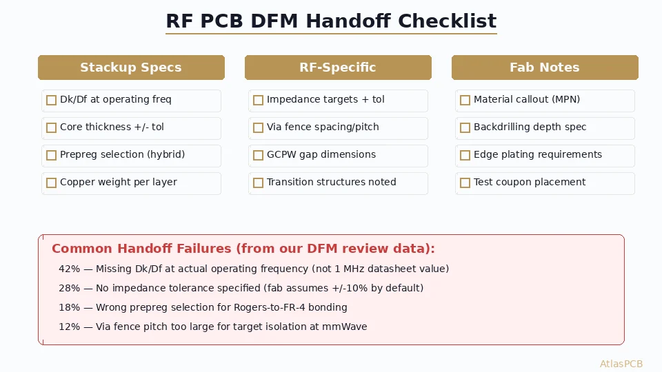
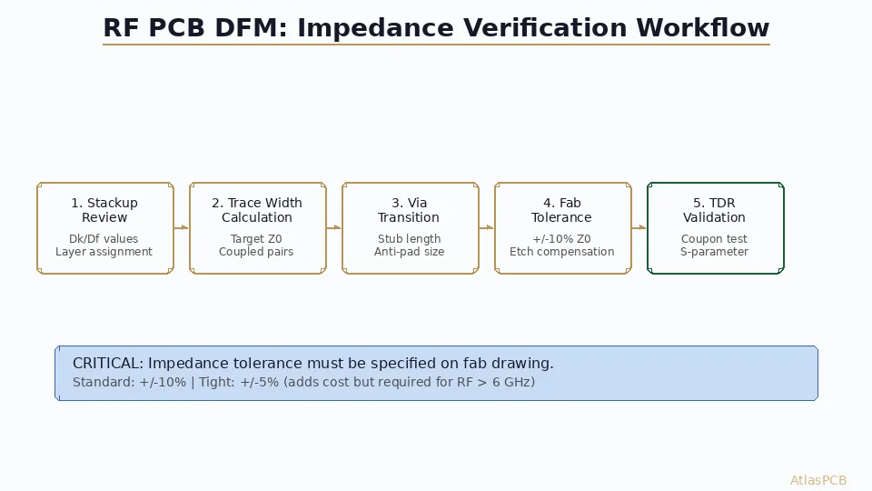
RF PCB DFM for impedance-controlled boards requires five verification steps before ordering: stackup Dk/Df validation against the specific laminate lot, trace width recalculation with manufacturer etch compensation, via transition stub analysis, fabrication tolerance specification on the drawing (+/-5% or +/-10%), and TDR coupon design for production verification. Most RF board re-spins trace back to Step 1 — using datasheet Dk values instead of manufacturer-specific process values that account for resin content variation.
Quick Answer: The Five-Step RF DFM Verification
| Step | Check | Common Error | Impact if Missed |
|---|---|---|---|
| 1. Stackup Dk/Df | Verify fabricator’s process Dk, not datasheet | Using 3.48 instead of 3.60 effective | 3-5 ohm impedance shift |
| 2. Trace Width | Recalculate with actual finished copper thickness | Ignoring plating buildup (+25um) | 2-4 ohm shift, marginal return loss |
| 3. Via Transition | Analyze stub length, specify backdrill if needed | 15+ mil stub at 10 GHz | 2-5 dB insertion loss per via |
| 4. Tolerance Spec | Explicit +/-X% on fab drawing with coupon reference | No tolerance specified | Manufacturer delivers +/-15% |
| 5. TDR Coupon | Define coupon structures matching critical traces | No production verification method | Impedance drift undetected across lots |
If you only fix one thing before ordering: get your fabricator’s actual characterized Dk value for your chosen material at your operating frequency. This single correction prevents more re-spins than all other DFM checks combined.
Step 1: Stackup Validation — The Dk Problem Nobody Tells You About
Every impedance calculator requires a dielectric constant input. Engineers naturally reach for the laminate manufacturer’s published Dk — Rogers lists 3.48 for RO4350B, Isola lists 3.67 for I-Tera MT40, Panasonic lists 3.40 for Megtron 6. These numbers are measured under specific conditions (10 GHz, clamped stripline, conditioned samples) that do not match your fabricated board.
The real Dk your signal sees depends on the complete fabricated structure: copper roughness profile (Rz of 3-6 um on standard copper adds 0.05-0.15 to effective Dk through the Hammerstad-Jensen model), resin content variation in the pressed stackup (more resin flow = lower effective Dk, but less predictable), glass weave style and orientation relative to your traces (the fiber bundle creates localized Dk variation of +/-0.05), and the fabricator’s specific pressing parameters (time, temperature, pressure profile affects final thickness and Dk homogeneity).
In our production facility, we maintain a characterized Dk database built from TDR measurements on production panels. For Rogers RO4350B processed with our standard press cycle, the effective Dk we use for impedance targeting is 3.62 at 5 GHz and 3.58 at 10 GHz — meaningfully different from the published 3.48. An engineer who calculates trace width using 3.48 and sends us the design will get boards 3-5 ohms low on impedance unless we catch it in DFM review and adjust.
The solution is straightforward: before finalizing your trace widths, ask your fabricator “what effective Dk value do you use for impedance targeting on [material] at [frequency]?” Any qualified RF PCB manufacturer maintains this data. If they cannot answer the question, they are not an RF-capable shop regardless of what materials they stock.
RF PCB ENGINEERING
Need Process-Validated Dk Values?
AtlasPCB maintains characterized dielectric constant tables for Rogers, Megtron, and PTFE laminates at multiple frequencies. We provide these values during DFM review.
Request Dk Data Sheet ›
Step 2: Trace Width Recalculation with Actual Copper Thickness
The second most common DFM error involves copper thickness assumptions. When you specify “1 oz copper” on your fab drawing, you get 35um of base copper foil. But outer-layer traces go through the plating process — first a thin electroless seed (1-2um), then electrolytic copper deposition to plate the vias. On outer layers, this adds 20-25um of plated copper on top of the 35um base, yielding 55-60um total finished copper thickness.
This matters because trace impedance is a function of trace width AND thickness. A 50-ohm microstrip trace on 8-mil RO4350B dielectric with 35um copper calculates to approximately 18.2 mil width. The same trace with 58um finished copper (after plating) requires only 16.8 mil — a 1.4 mil difference. If you designed at 18.2 mil and the fabricator builds with their normal plating thickness, your impedance comes in at 46-47 ohms.
The proper workflow: specify finished copper thickness (not base copper weight) in your impedance calculation. On your fab drawing, add a note: “Impedance calculation based on finished copper thickness of 58um (outer) and 35um (inner). Fabricator to target specified trace widths; do not apply etch compensation to impedance-controlled nets without engineering approval.”
Some fabricators will apply their own etch compensation — widening traces slightly to account for the lateral etch that narrows them during processing. This is correct for non-impedance traces but can create confusion on impedance-controlled lines where the designer already accounted for the process. Clear communication on the fab drawing prevents this.
Step 3: Via Transition — The Hidden Impedance Killer Above 6 GHz
Below 3 GHz, via stubs are rarely a concern. The stub resonance frequency of a typical 62-mil (1.57mm) board occurs around 24 GHz for a full-length stub — well above most designs. But as operating frequencies push into the 6-28 GHz range for 5G, automotive radar, and satellite communications, stub management becomes critical.
A via carrying signal from Layer 1 (top) to Layer 3 (inner stripline) leaves a stub extending from Layer 3 down to the bottom of the board. On a 93-mil (2.36mm) 10-layer board with signal on Layer 3, the stub length is approximately 70 mil (1.78mm). This stub resonates at roughly 10.5 GHz (quarter-wave in FR-4), creating a notch filter that can eat 5-10 dB of your signal right in the operating band.
The solutions, in order of preference and cost:
Backdrilling (most common for production): The fabricator drills out the stub with a larger-diameter drill bit after plating, leaving a controlled residual stub of 5-8 mil. This is routine at most competent manufacturers and adds 10-20% to the via processing cost. Specify backdrill on your drawing as: “Backdrill all signal vias on layers [X] to residual stub length of 8 mil max (+/-3 mil). Backdrill diameter: 0.35mm.”
Blind/buried vias (highest performance): Eliminate the stub entirely by using a blind via from the surface to the target layer only. More expensive (adds 30-50% to board cost due to sequential lamination) but provides the best electrical performance and saves routing real estate.
Via-in-pad with stub control (compact designs): For BGA breakout where you cannot backsdrill due to component mounting on both sides, use controlled-depth blind vias for critical signals and accept through-hole vias only for low-frequency connections (power, I2C, reset lines).
In our production, we achieve backdrill accuracy of +/-3 mil residual stub, verified by cross-section on coupon vias for each panel. This specification should appear on your fab drawing for any design operating above 6 GHz with through-hole signal vias.
IMPEDANCE CONTROL
Designing for 6+ GHz? Get DFM Review First
Our RF engineers review stackup, via transitions, and backdrill specifications before fabrication. We catch the issues that cause expensive re-spins.
Step 4: Fabrication Tolerance Specification
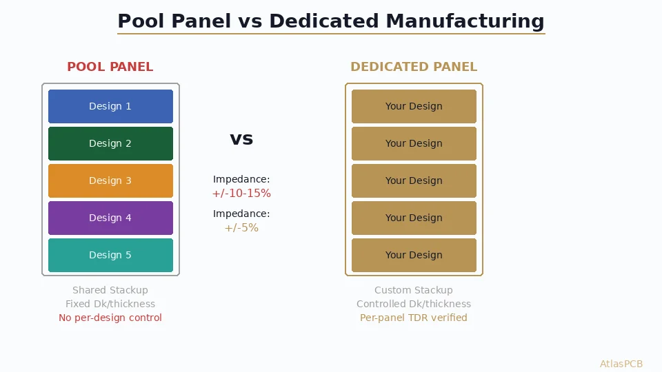
Impedance tolerance is not implied — you must specify it explicitly on your fab drawing or you receive whatever the manufacturer’s process naturally delivers. Standard manufacturing without special controls yields approximately +/-12-15% impedance variation. With controlled processes (LDI imaging, monitored pressing, etch factor compensation), +/-10% is routine and +/-5% is achievable with premium pricing.
The tolerance you need depends entirely on your link budget analysis. For a 10 Gbps NRZ link with 15 dB of insertion loss budget and healthy margins, +/-10% impedance tolerance contributes only 0.3-0.5 dB of additional reflection loss — negligible. For a 56 Gbps PAM4 link operating at its sensitivity limit with 2 dB of margin, that same +/-10% variation can consume your entire margin through accumulated reflections at multiple via transitions and connector interfaces.
How to specify on your fab drawing:
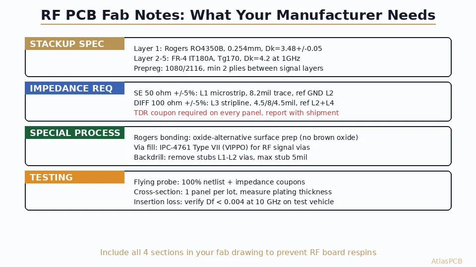
Add an impedance control table with columns for: net class name, impedance target (ohms), tolerance (+/-%), layer(s), line type (microstrip/GCPW/stripline/differential), and reference standard (typically IPC-TM-650 2.5.5.7). Include a note referencing the impedance test coupon location in your panel border.
Example table entry:
- NET_CLASS: RF_50OHM | Target: 50 ohm | Tol: +/-5% | Layer: L1 | Type: GCPW | Ref: Coupon A
- NET_CLASS: DIFF_100 | Target: 100 ohm differential | Tol: +/-7% | Layers: L3-L4 | Type: Edge-coupled stripline | Ref: Coupon B
Step 5: TDR Coupon Design for Production Verification
The impedance test coupon is your only verification that production boards meet your specification across the entire production run. Coupons are short transmission line segments (typically 6-8 inches long) fabricated in the panel border using the same trace widths, layer assignments, and process steps as your board.
Key coupon design rules that many engineers miss:
Match your actual trace configuration. If your board uses coplanar waveguide (GCPW) with 5-mil gap to ground flood, your coupon must replicate that exact geometry — not just a bare microstrip. The coplanar ground proximity changes impedance by 3-8 ohms depending on gap width.
Include all critical line types. One coupon per unique impedance class — you cannot verify 50-ohm microstrip and assume 100-ohm differential stripline is also correct, because they have different sensitivity to dielectric thickness variation.
Specify the measurement method. TDR (Time Domain Reflectometry) per IPC-TM-650 2.5.5.7 is standard. Note: TDR results include fixture effects (probe launch, connector) that add 1-2 ohms of apparent impedance. Specify whether the reported value should include or exclude fixture de-embedding.
At AtlasPCB, we measure every production panel’s coupons using calibrated TDR with fixture de-embedding. Results are documented in the inspection report alongside cross-section photos showing actual trace dimensions. If a panel measures outside tolerance, it is either reworked (etch adjustment on subsequent panels) or scrapped — it does not ship.
CHINA RF PCB MANUFACTURER
Impedance-Controlled Boards with TDR Verification
Every RF order includes TDR coupon measurement with calibrated de-embedding. We stock Rogers RO4350B, Megtron 6, and PTFE laminates for immediate production start.
Get RF PCB Quote ›Common DFM Errors by Application Frequency
| Frequency Range | Top DFM Issue | How We Catch It |
|---|---|---|
| DC-1 GHz | Wrong copper thickness assumption | Cross-reference finished Cu with impedance calc |
| 1-6 GHz | Incorrect Dk value (datasheet vs process) | Compare designer’s calc against our characterized Dk |
| 6-15 GHz | Uncontrolled via stubs (no backdrill spec) | Flag signal vias with stub > 10 mil |
| 15-28 GHz | Glass weave effect on trace impedance | Recommend spread glass or rotated routing |
| 28+ GHz | Surface roughness dominating loss | Specify HVLP or UHVLP foil; validate loss budget |
Each frequency range introduces additional process requirements. The critical insight: a board that works perfectly at 2.4 GHz may fail catastrophically at 10 GHz from effects that simply do not matter at lower frequencies. Your DFM review must be frequency-aware.
ATLASPCB
Submit Your RF Design for Expert DFM Review
Our process engineers validate stackup, impedance calculations, via transitions, and material selection before production. Impedance-controlled boards from 1-30 layers with Rogers, Megtron, and PTFE materials.
Upload Gerbers for Review ›
Reviewed by AtlasPCB Engineering Team — 15+ years in advanced PCB fabrication for RF, HDI, and rigid-flex applications.
Related Reading:
About AtlasPCB — We specialize in complex PCB manufacturing for HDI, RF, and high-reliability applications. Explore our RF and high-frequency PCB services, impedance-controlled PCB manufacturing, or get an free engineering DFM review . Every order includes free engineering review. Get your quote.
Reviewed by AtlasPCB Engineering Team — IPC-certified manufacturing specialists with 15+ years of production experience in HDI, RF, and high-reliability PCB fabrication. Content based on factory floor data and real customer design reviews.
Frequently Asked Questions
What Dk value should I use for impedance calculation on Rogers 4350B?
What impedance tolerance should I specify for RF boards?
How do I specify impedance on a PCB fab drawing?
What is the most common RF PCB DFM error?
Should I use microstrip or stripline for RF signals?
- RF PCB design and manufacturing
- impedance controlled PCB manufacturer
- PCB DFM check
- China RF PCB manufacturer