· AtlasPCB Engineering · Engineering · 22 min read
12-Layer PCB Stackup Design: Configurations, Impedance Control, and Cost Optimization Guide
A manufacturer's guide to 12-layer PCB stackup design covering three proven configurations with specific prepreg and core dimensions, impedance control methodology, HDI vs through-hole construction, DFM pitfalls from our production floor, and detailed cost analysis comparing 10-layer and 16-layer alternatives.

Quick Answer
A 12-layer PCB stackup typically uses 5-7 signal layers and 5-7 plane layers (ground + power), built from 5 core laminates and 6 prepreg layers to a standard finished thickness of 1.6mm or 2.0mm. The three most common configurations are: signal-integrity-optimized (5 signal / 4 ground / 3 power), routing-dense (7 signal / 3 ground / 2 power), and mixed-signal isolation (5 signal / 5 ground / 2 power). Cost is typically 25-35% more than a 10-layer board and 30-40% less than a 16-layer board at prototype quantities. The primary cost drivers beyond layer count are whether HDI construction (1+10+1) is required, material grade selection, and impedance tolerance requirements.
When a 10-Layer Board Is No Longer Enough
The decision to move from a 10-layer PCB stackup to a 12-layer design should be driven by specific, quantifiable constraints rather than a vague sense that more layers will solve routing problems. In our fabrication facility, 12-layer boards represent approximately 12% of orders above 8 layers, and the engineering justifications follow predictable patterns that we can describe with precision.
The most common trigger is high-speed interface proliferation beyond what five signal layers can accommodate with proper reference plane discipline. A well-designed 10-layer board provides four to five signal layers, each adjacent to a continuous ground reference. When a design simultaneously carries DDR5 at 4800MT/s across two channels, PCIe Gen5 x8, multiple USB4 links, and a 25GbE SerDes interface, each bus ideally demands its own dedicated routing layer with tight coupling to an unbroken ground plane. At 10 layers, designers face an uncomfortable choice: either share signal layers between protocols operating at different speeds (risking crosstalk coupling between 4800MT/s DDR strobes and 32GT/s PCIe lanes) or route some signals without an immediately adjacent ground reference, degrading return-path continuity at frequencies where every discontinuity becomes an antenna.
The second trigger involves BGA escape complexity. Modern SoCs and FPGAs with 800 to 1500 balls at 0.65mm or 0.8mm pitch generate escape routing demands that overwhelm five signal layers. The inner rows of a 1000-pin BGA at 0.8mm pitch require four to five routing channels between pads, and when two or three such packages share a board with limited escape area, the congestion cannot be resolved without additional signal layers. Adding two layers through the 12-layer configuration provides the routing capacity to fan out these packages while maintaining 4/4mil minimum trace-and-space rules and avoiding via-in-pad on every single pad.
The third scenario involves power distribution complexity in designs with five or more voltage domains at moderate current. Modern FPGA and processor designs frequently require 0.85V core, 1.2V I/O, 1.8V auxiliary, 2.5V SerDes, 3.3V legacy, and sometimes 5V for interface transceivers. Attempting to distribute all these rails on two power planes forces extensive plane splitting, which creates discontinuities in the return current path wherever a high-speed signal crosses a split boundary. A 12-layer stackup can dedicate three full power planes to voltage distribution while maintaining four ground planes, eliminating the need for aggressive plane splitting.
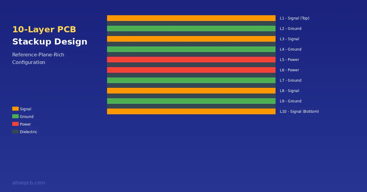
From a manufacturing standpoint, the transition from 10 to 12 layers adds one additional core laminate and one more prepreg layer to the book. The same lamination presses, drilling equipment, and imaging lines handle both layer counts. The incremental cost comes from additional material, a slightly longer press cycle, and the tighter registration requirements that come with managing twelve copper layers through multiple process steps.
Not sure whether you need 10 or 12 layers?
Upload your schematic or preliminary layout and our engineers will analyze your routing density, signal speed requirements, and power distribution needs. We will recommend the optimal layer count with a detailed stackup proposal showing exact prepreg and core selections for your impedance targets. Free with every quote request.
Get a Free Stackup ReviewThree Proven 12-Layer Stackup Configurations
Every 12-layer PCB design begins with an architectural decision about how to distribute signal, ground, and power layers across twelve copper planes. This choice determines which signals will have ideal reference planes, how power distribution performs at high frequencies, and what manufacturing tolerances the fabricator must hold. After producing tens of thousands of 12-layer panels across networking, server, automotive, and telecommunications applications, we have identified three configurations that address the vast majority of design requirements.
Configuration A: Signal-Integrity-Optimized (5 Signal / 4 Ground / 3 Power)
This is our recommended configuration for high-speed digital designs where signal integrity takes absolute priority. The architecture places four continuous ground planes such that every signal layer has an immediately adjacent ground reference, creating ideal stripline geometry for controlled impedance routing on all inner signal layers.
| Layer | Function | Copper Weight | Reference | Dielectric Below |
|---|---|---|---|---|
| L1 (Top) | Signal + Components | 1oz (35um) | Microstrip to L2 GND | 3.5mil 1080 prepreg (Dk 4.2) |
| L2 | Continuous Ground | 0.5oz (17um) | — | 4.0mil core (Dk 4.4) |
| L3 | Signal (High-Speed) | 0.5oz (17um) | Stripline L2/L4 GND | 4.0mil 1080 prepreg (Dk 4.2) |
| L4 | Continuous Ground | 0.5oz (17um) | — | 4.5mil core (Dk 4.4) |
| L5 | Signal (High-Speed) | 0.5oz (17um) | Stripline L4 GND/L6 PWR | 4.0mil 2116 prepreg (Dk 4.2) |
| L6 | Power Plane 1 | 1oz (35um) | — | 4.0mil core (Dk 4.4) |
| L7 | Power Plane 2 | 1oz (35um) | — | 4.0mil 2116 prepreg (Dk 4.2) |
| L8 | Signal (High-Speed) | 0.5oz (17um) | Stripline L7 PWR/L9 GND | 4.5mil core (Dk 4.4) |
| L9 | Continuous Ground | 0.5oz (17um) | — | 4.0mil 1080 prepreg (Dk 4.2) |
| L10 | Signal (High-Speed) | 0.5oz (17um) | Stripline L9/L11 GND | 4.0mil core (Dk 4.4) |
| L11 | Continuous Ground + Power 3 | 0.5oz (17um) | — | 3.5mil 1080 prepreg (Dk 4.2) |
| L12 (Bottom) | Signal + Components | 1oz (35um) | Microstrip to L11 GND | — |
Total finished thickness: approximately 1.6mm (63mil). This construction uses 1080 glass style prepreg on the outer dielectric layers for tight microstrip impedance control (50-ohm single-ended at 4.2mil trace width) and 2116 glass style in the center for structural stability during lamination.
The key advantage of Configuration A is that layers 3, 5, 8, and 10 all operate as ground-referenced stripline with continuous copper planes on both sides. This geometry provides impedance tolerance within plus or minus 7% without requiring premium manufacturing controls, and the shielding effect of adjacent ground planes suppresses crosstalk between signal layers to below -50dB at 10GHz for traces separated by a single ground plane.
The trade-off is routing capacity: five signal layers (plus two component-side microstrip layers) provides adequate channel count for most designs with 2000-3500 nets, but designs exceeding this density may need Configuration B.
Configuration B: Routing-Dense (7 Signal / 3 Ground / 2 Power)
When routing density is the primary constraint and signal speeds remain below 10 Gbps, this configuration maximizes the number of available signal layers while maintaining acceptable signal integrity.
| Layer | Function | Copper Weight | Reference | Dielectric Below |
|---|---|---|---|---|
| L1 (Top) | Signal + Components | 1oz (35um) | Microstrip to L2 GND | 3.5mil 1080 prepreg |
| L2 | Continuous Ground | 0.5oz (17um) | — | 3.5mil core |
| L3 | Signal | 0.5oz (17um) | Stripline L2 GND/L4 | 3.5mil 1080 prepreg |
| L4 | Signal | 0.5oz (17um) | Ref to L2 GND (offset) | 3.5mil core |
| L5 | Power Plane 1 | 1oz (35um) | — | 4.0mil 2116 prepreg |
| L6 | Continuous Ground | 0.5oz (17um) | — | 4.0mil core |
| L7 | Continuous Ground | 0.5oz (17um) | — | 4.0mil 2116 prepreg |
| L8 | Power Plane 2 | 1oz (35um) | — | 3.5mil core |
| L9 | Signal | 0.5oz (17um) | Ref to L10 GND (offset) | 3.5mil 1080 prepreg |
| L10 | Signal | 0.5oz (17um) | Stripline L9/L11 GND | 3.5mil core |
| L11 | Continuous Ground | 0.5oz (17um) | — | 3.5mil 1080 prepreg |
| L12 (Bottom) | Signal + Components | 1oz (35um) | Microstrip to L11 GND | — |
This configuration provides seven usable signal layers but introduces a compromise: layers 4 and 9 reference a ground plane that is not immediately adjacent (offset stripline geometry). This increases impedance sensitivity to manufacturing tolerances and raises the crosstalk floor between L3/L4 and L9/L10 pairs. We recommend this configuration only when signal rise times exceed 200ps (corresponding to bandwidths below approximately 5GHz) and when routing congestion genuinely cannot be resolved with five signal layers.
Configuration C: Mixed-Signal Isolation (5 Signal / 5 Ground / 2 Power)
For designs combining sensitive analog, RF, and noisy digital sections on a single board, this configuration prioritizes ground plane isolation between signal domains.
| Layer | Function | Copper Weight | Reference | Dielectric Below |
|---|---|---|---|---|
| L1 (Top) | Signal - Digital | 1oz (35um) | Microstrip to L2 GND | 3.5mil 1080 prepreg |
| L2 | Ground (Digital) | 0.5oz (17um) | — | 4.0mil core |
| L3 | Signal - Digital High-Speed | 0.5oz (17um) | Stripline L2/L4 GND | 4.0mil 1080 prepreg |
| L4 | Ground (Isolation) | 0.5oz (17um) | — | 4.0mil core |
| L5 | Power Plane (Digital) | 1oz (35um) | — | 5.0mil 2116 prepreg |
| L6 | Ground (Center Shield) | 1oz (35um) | — | 5.0mil 2116 prepreg |
| L7 | Power Plane (Analog) | 1oz (35um) | — | 4.0mil core |
| L8 | Ground (Isolation) | 0.5oz (17um) | — | 4.0mil 1080 prepreg |
| L9 | Signal - Analog/RF | 0.5oz (17um) | Stripline L8/L10 GND | 4.0mil core |
| L10 | Ground (Analog) | 0.5oz (17um) | — | 4.0mil 1080 prepreg |
| L11 | Signal - Analog/RF | 0.5oz (17um) | Stripline L10/L12 GND | 3.5mil core |
| L12 (Bottom) | Signal - Analog + Components | 1oz (35um) | Microstrip to L10 GND | — |
The defining feature of Configuration C is the continuous ground plane on Layer 6 that acts as a shield between the digital domain (L1-L5) and the analog/RF domain (L7-L12). This provides greater than 60dB isolation between domains at frequencies up to 6GHz, which is critical for mixed-signal designs such as software-defined radio platforms, medical imaging front-ends, and precision measurement instruments where digital switching noise must not contaminate analog signal paths.
Impedance Control in 12-Layer Designs
Impedance control on a 12-layer board follows the same physics as any multilayer PCB, but the additional layers create both opportunities and challenges that warrant specific discussion. With twelve copper planes available, designers can place every high-speed signal in an ideal stripline geometry between two continuous reference planes, achieving tighter impedance tolerance than is practical on 6- or 8-layer boards where some signals inevitably route as offset-referenced stripline or edge-coupled microstrip.
For Configuration A, the standard impedance targets and achievable trace geometries are as follows. A 50-ohm single-ended microstrip on L1 referenced to L2 ground with 3.5mil dielectric spacing requires a trace width of approximately 4.2mil at 1oz copper thickness and Dk of 4.2. The same 50-ohm target in stripline geometry on L3 (referenced to L2 and L4 ground planes each 4.0mil away) requires approximately 3.8mil trace width at 0.5oz copper. For 100-ohm differential pairs in stripline, the typical geometry is 4.0mil trace width with 5.0mil gap between pairs, referenced to ground planes 4.0mil away on both sides.
The manufacturing tolerance for impedance on a 12-layer board is typically plus or minus 10% for standard process and plus or minus 7% for controlled impedance with coupon verification. The tighter tolerance is achievable because stripline geometry is inherently more stable than microstrip: both reference planes constrain the electromagnetic field, making the impedance less sensitive to variations in copper plating thickness or solder mask profile that affect outer-layer microstrip traces.
One critical consideration specific to 12-layer designs is the prepreg selection for layers where impedance tolerance is tightest. We recommend 1080 glass style prepreg (single ply, 3.3-3.7mil pressed thickness) for signal-to-ground spacings below 4mil because its thin profile provides the dielectric uniformity needed for consistent impedance. For spacings above 4mil, 2116 glass style (single ply, 4.5-5.0mil pressed thickness) or two plies of 1080 provide better thickness uniformity across the panel area.
The relationship between trace width tolerance and impedance variation deserves attention in the 12-layer context. Inner-layer etching on modern lines holds trace width to plus or minus 0.5mil (12.5 microns). On a 4.0mil nominal trace in stripline, this 0.5mil variation produces approximately 5% impedance shift. Combined with the 3-5% variation from dielectric thickness tolerance, the total impedance spread falls within the plus or minus 10% budget without difficulty. This is why specifying impedance on your fab drawing matters more than specifying exact trace widths: let the fabricator adjust trace geometry during DFM review to hit your impedance target given their actual material lot properties.
Need impedance-controlled 12-layer boards?
We provide free impedance modeling with every 12-layer quote. Send us your stackup requirements and target impedances, and our engineers will deliver a complete stackup proposal with trace width calculations, prepreg selections, and TDR coupon design included at no charge.
Request Impedance ModelingStandard Through-Hole vs HDI 12-Layer Construction
A 12-layer PCB can be built in two fundamentally different ways: conventional through-hole construction where all twelve layers are laminated simultaneously and vias are mechanically drilled through the entire board thickness, or HDI construction with sequential lamination that adds buildup layers with laser-drilled microvias.
The most common HDI variant for 12 layers is the 1+10+1 structure. In this construction, a 10-layer core is manufactured first using conventional processes, then one additional copper layer is laminated onto each side with laser-drilled microvias connecting the buildup layer to the adjacent core layer. This provides all the benefits of microvias on the outer layers (enabling 0.4mm pitch BGA escape without through-hole via-in-pad) while keeping the inner 10 layers in conventional construction.
The cost differential between these approaches is significant. Standard through-hole 12-layer construction uses a single lamination cycle and mechanical drilling only. HDI 1+10+1 requires three lamination cycles (10-layer core lamination plus two sequential laminations for the buildup layers), laser drilling equipment for the microvias, and additional imaging and plating steps for the buildup layers. In practice, this translates to a 40-60% cost premium for HDI 1+10+1 over standard 12-layer at our facility, with lead time extending by 3-5 working days.
The decision between standard and HDI construction depends primarily on component pitch. If all BGAs use 0.8mm pitch or larger, through-hole construction with standard 0.3mm (12mil) drill and dog-bone fanout is almost always sufficient and far more economical. When any component uses 0.5mm or 0.4mm pitch, HDI microvias become necessary for escape routing, and the 1+10+1 structure is the cost-efficient way to add that capability without moving to a full any-layer HDI construction. For a detailed HDI cost analysis, we have published separate pricing guidance.
Material Selection by Application
The choice of laminate material for a 12-layer PCB should be driven by the highest-speed interface on the board, not by the average signal speed. A single 28 Gbps NRZ SerDes link determines the material requirement for the entire stackup, even if 90% of the nets operate at low speed.
For designs where all signals operate below 5 Gbps (most industrial controllers, automotive body electronics, and general embedded systems), standard FR-4 with Tg 170 degrees Celsius provides adequate performance at the lowest material cost. The dielectric constant of 4.2-4.5 and loss tangent of 0.018-0.022 at 1GHz are acceptable for these speeds, and the material is available from every laminate supplier with consistent properties and short lead times.
When signal speeds reach 10-16 Gbps (PCIe Gen4, 10GbE, USB4 Gen2), a mid-loss material like Isola 370HR or Panasonic Megtron 4 becomes necessary. These materials offer loss tangent of 0.012-0.015 at 1GHz and more stable Dk across frequency, reducing insertion loss on long traces by 25-35% compared to standard FR-4. The cost premium is approximately 15-25% over standard FR-4 for the raw material, with no change to manufacturing process parameters.
For designs pushing 25-56 Gbps per lane (PCIe Gen5/Gen6, 400GbE, advanced AI accelerator interconnects), low-loss materials such as Panasonic Megtron 6 (Df 0.004 at 12GHz) or Megtron 7 (Df 0.002 at 12GHz) are required. These materials cost 2-3x more than standard FR-4 but are essential for maintaining open eye diagrams at these data rates over trace lengths exceeding 3 inches. A hybrid approach using low-loss material on signal-layer dielectrics and standard FR-4 on power-plane dielectrics can reduce cost by 20-30% while maintaining signal performance, since insertion loss is dominated by the dielectric adjacent to the signal trace.
For RF applications requiring precise Dk control and extremely low loss, Rogers 4350B (Dk 3.48, Df 0.0037) or PTFE-based laminates can be incorporated as hybrid layers within an otherwise FR-4 stackup. In a 12-layer board, this might mean placing Rogers material on the core between L3 and L4 where RF traces route, while using FR-4 everywhere else. This hybrid approach requires careful CTE matching at the material boundaries to prevent delamination during thermal cycling.
Manufacturing Process and Yield Considerations
A 12-layer PCB moves through essentially the same manufacturing sequence as any multilayer board, but the additional layers compound certain process challenges that affect yield and require tighter process controls.
Inner-layer fabrication begins with imaging and etching all ten inner copper layers simultaneously on five double-sided core panels. Each core is individually inspected using automated optical inspection to verify trace width, spacing, and registration accuracy. At 12 layers, the statistical probability of at least one inner layer having a defect increases compared to 8 or 10 layers. If inner-layer yield per layer is 98.5% (typical for a well-controlled process), the probability of a perfect set of 10 inner layers is 0.985 to the tenth power, which equals approximately 86%. This means that roughly 14% of panels require repair or replacement of at least one inner layer before lamination proceeds.
Registration accuracy becomes more demanding as layer count increases. Each layer must align to a common reference system (typically tooling holes or optical targets) with sufficient accuracy that all twelve layers maintain their intended spatial relationship after lamination. For a 12-layer board with 4/4mil trace and space design rules, the layer-to-layer registration tolerance is typically specified at plus or minus 2mil (50 microns), and the total registration from any layer to any other layer must remain within plus or minus 3mil (75 microns). Achieving this requires precise pin-lamination or optical registration systems during layup, and careful control of material movement during the lamination press cycle.
Drill aspect ratio presents a specific challenge for 12-layer boards at 1.6mm finished thickness. The smallest standard mechanical drill for through-hole vias is 0.2mm (8mil), which at 1.6mm board thickness produces an aspect ratio of 8:1. This is at the limit of reliable copper plating for most electroplating processes. Plating solution struggles to reach the center of high-aspect-ratio holes uniformly, potentially creating voids or thin spots in the barrel plating that compromise reliability during thermal cycling. For this reason, we recommend a minimum via drill size of 0.25mm (10mil) for 12-layer boards at 1.6mm thickness, producing a more comfortable 6.4:1 aspect ratio that reliably plates with greater than 25 microns of copper in the barrel center.
Lamination parameters for 12-layer boards require careful optimization. The press cycle must achieve sufficient resin flow to fill all inner-layer copper features and eliminate voids, while avoiding excessive flow that would thin the prepreg below its target pressed thickness. With twelve copper layers creating more surface topography than a thinner stackup, the press cycle typically runs at higher pressure (350-400 PSI versus 300 PSI for 8-layer boards) and slightly longer dwell time at peak temperature to ensure complete resin cure throughout the thicker book.
Common DFM Mistakes on 12-Layer Orders
After reviewing thousands of 12-layer designs submitted for fabrication, certain mistakes recur with predictable frequency. Understanding these common errors before submitting Gerbers can save an entire design revision cycle.
The first and most frequent mistake is specifying via drill sizes that create excessive aspect ratios. Designers accustomed to 8-layer boards at 1.6mm thickness routinely use 0.2mm (8mil) vias, which work reliably at 8:1 aspect ratio on those thinner stackups. On a 12-layer board at the same 1.6mm thickness, those same vias still produce 8:1 aspect ratio, but the additional thermal cycling stress from twelve copper layers expanding and contracting makes reliability marginal. More critically, designers who move to 2.0mm finished thickness for their 12-layer board without adjusting via size create 10:1 aspect ratios that exceed our plating capability. The fix is straightforward: use 0.25mm minimum drill for 1.6mm boards and 0.3mm minimum drill for 2.0mm boards.
The second common mistake is placing high-speed signal layers adjacent to power planes with splits rather than continuous ground planes. In a 12-layer stackup, designers sometimes route a 10+ Gbps signal on a layer referenced to a power plane that contains splits between different voltage domains. When the signal trace crosses the plane split, the return current must detour around the split, creating a slot antenna that radiates EMI and causes impedance discontinuity at the crossing point. This produces a localized impedance spike of 10-20% and can cause the board to fail radiated emissions testing. The solution is to ensure all layers carrying signals above 5 Gbps reference only continuous, unsplit ground planes.
The third mistake involves stackup asymmetry that causes warpage during reflow soldering. A 12-layer stackup must be symmetric about its center line in terms of copper distribution, dielectric thickness, and material type. We regularly receive designs where the top half of the stackup uses different prepreg thicknesses than the bottom half, or where copper distribution is heavier on one side (more power planes above center, more signal layers below center). During reflow soldering at 260 degrees Celsius peak temperature, asymmetric stackups develop bow and twist that can exceed IPC-6012 limits (0.75% for surface mount boards), causing component placement failures and solder joint reliability issues.
The fourth mistake is inadequate clearance between via anti-pads and impedance-controlled traces on inner layers. On a 12-layer board with five or six signal layers, routing density is typically high enough that traces must pass between via anti-pads on the reference planes. If a ground-referenced trace passes within 8mil of a via anti-pad on its reference ground plane, the local removal of ground copper changes the effective trace-to-reference distance, creating an impedance bump. With hundreds of vias per square inch on a dense 12-layer design, these anti-pad interactions accumulate and can push aggregate impedance variation beyond specification. We recommend maintaining at least 10mil clearance between impedance-critical traces and via anti-pad edges, or specifying reduced anti-pad diameter (minimum 16mil larger than drill) to minimize the ground copper removal.
The fifth mistake is failing to account for copper balancing across all twelve layers. Uneven copper distribution between layers creates differential stress during lamination and thermal processing, leading to internal delamination or measurable warpage. The target is to keep copper coverage on each layer within a 20% range (for example, if the densest layer has 70% copper fill, no layer should fall below 50%). Adding copper thieving patterns or ground fill on sparse signal layers is the standard remedy, but designers sometimes forget to apply this to all twelve layers rather than just the outer two.
Avoid costly re-spins with a free DFM review
Submit your 12-layer design files and our engineering team will check for all five common mistakes listed above, plus 40+ additional DFM rules specific to your layer count and material selection. We catch stackup issues before they become fabrication failures.
Submit for Free DFM ReviewCost Analysis: 12-Layer vs Alternatives
Understanding the cost structure of a 12-layer PCB requires examining both the absolute cost and the relative premium compared to adjacent layer counts. The following analysis is based on our current pricing for a representative board specification: 100mm x 100mm, 1oz outer copper, 0.5oz inner copper, FR-4 Tg170, ENIG surface finish, green solder mask, and standard impedance control (plus or minus 10%).
At prototype quantities (5-10 pieces), the pricing comparison across layer counts looks approximately as follows. An 8-layer board at this specification costs $35-50 per board. A 10-layer board costs $55-80 per board. A 12-layer board costs $70-105 per board. A 16-layer board costs $120-170 per board. The cost jump from 10 to 12 layers (25-35%) is smaller than the jump from 12 to 16 layers (70-65%), because the step from 12 to 16 adds four layers rather than two, and 16-layer boards often require tighter registration tolerances that reduce manufacturing yield.
At production quantities (1000+ pieces), the cost differential narrows because material cost becomes the dominant factor. Material scales linearly with layer count (two additional copper foils, one additional core, one additional prepreg sheet), while setup and handling costs are amortized across many panels. The 12-layer premium over 10-layer at production volumes is typically 15-25%, and the premium over 8-layer is approximately 35-50%.
Several design choices affect 12-layer cost beyond the base layer count. Specifying controlled impedance with plus or minus 7% tolerance (versus the standard plus or minus 10%) adds approximately 10-15% for the additional process controls and coupon testing. Choosing Megtron 6 instead of FR-4 Tg170 adds 80-120% to material cost (approximately 25-40% to total board cost). Adding HDI 1+10+1 construction adds 40-60% over standard through-hole 12-layer. Specifying Class 3 IPC-6012 acceptance criteria adds 15-25% for the additional inspection requirements and lower acceptance threshold for defects.
The cost-optimization strategy for 12-layer boards focuses on three levers. First, maximize panel utilization by choosing board dimensions that array efficiently on standard panel sizes (18x24 inch or 21x24 inch working areas). Second, keep via drill sizes at 0.25mm or larger to avoid the yield impact of high aspect ratios. Third, avoid mixing material types within the stackup unless signal integrity absolutely requires it, because hybrid material handling adds setup time and increases material waste.
When to Choose 12 Layers: Decision Matrix
The following decision framework provides quantified thresholds for choosing between common layer counts. These thresholds assume standard complexity components and typical routing density requirements.
| Decision Criteria | 8 Layers | 10 Layers | 12 Layers | 16 Layers |
|---|---|---|---|---|
| Total net count | Under 1500 | 1500-2500 | 2500-4500 | Above 4500 |
| Maximum signal speed | Under 5 Gbps | 5-16 Gbps | 16-56 Gbps | Above 56 Gbps |
| BGA pin count (largest) | Under 500 | 500-800 | 800-1500 | Above 1500 |
| Number of BGAs | 1-2 | 2-3 | 3-5 | Above 5 |
| High-speed interfaces | 1-2 | 2-4 | 4-6 | Above 6 |
| Voltage domains | 2-3 | 3-5 | 5-8 | Above 8 |
| Required signal layers | 3-4 | 4-5 | 5-7 | Above 7 |
| Required plane layers | 4 | 5-6 | 5-7 | Above 7 |
| Cost index (prototype) | 1.0x | 1.5x | 2.0x | 3.5x |
| Typical lead time | 5-7 days | 7-10 days | 10-14 days | 14-21 days |
These thresholds represent typical boundaries, not absolute rules. A design with 2000 nets but four high-speed SerDes channels at 25 Gbps might need 12 layers even though net count alone suggests 10 layers are sufficient. Conversely, a design with 3000 nets but all signals below 1 Gbps and no tight impedance requirements might fit comfortably on 10 layers with aggressive routing optimization.
The most reliable decision method is to attempt routing on the lower layer count first. If routing completion stalls below 95% with design rule violations concentrated in BGA escape regions or high-speed interface areas, the design is telling you that additional layers are needed. Starting the layout at 12 layers when 10 might suffice wastes the cost differential on every production run for the lifetime of the product.
Ready to order your 12-layer PCB?
Get a detailed quote with stackup proposal, impedance modeling, and DFM review included. Our engineering team specializes in high-layer-count boards for networking, server, and high-speed digital applications. Typical lead time for 12-layer prototypes is 10-14 working days with express options available.
Get Your 12-Layer QuoteRelated Resources
For additional guidance on multilayer PCB stackup design, refer to our complete series covering different layer counts and related manufacturing considerations:
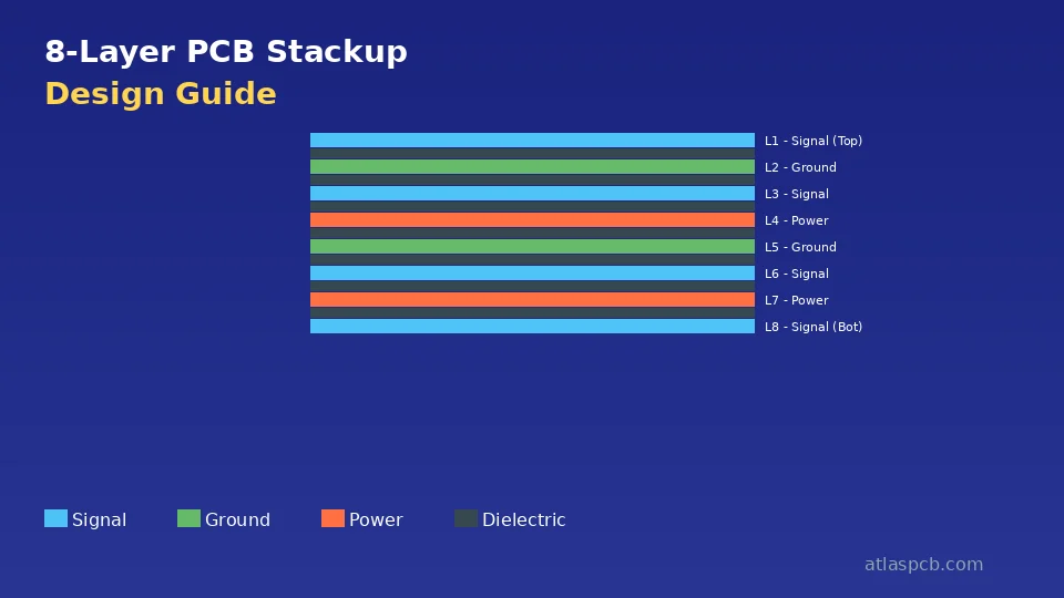
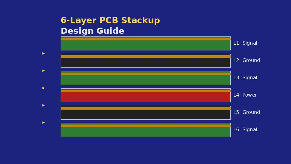
- 6-Layer and 8-Layer PCB Stackup Design Guide covers the fundamentals of layer assignment for boards where every layer matters.
- 10-Layer PCB Stackup Design Guide details the configurations and cost analysis for the layer count immediately below 12 layers.
- The 10-to-12 Layer Cost Jump explains specifically why the price increase occurs and how to minimize it through design optimization.
- How to Specify Impedance Control on Your Fab Drawing provides templates and examples for communicating impedance requirements to your manufacturer.
- Prepreg Selection Guide covers glass weave styles, resin content, and their effect on impedance control in detail.
About AtlasPCB — We specialize in complex PCB manufacturing for HDI, RF, and high-reliability applications. Explore our HDI PCB manufacturing capabilities, impedance-controlled PCB manufacturing, or get an Megtron 6 & 7 low-loss PCB manufacturing . Every order includes free engineering review. Get your quote.
Reviewed by AtlasPCB Engineering Team — IPC-certified manufacturing specialists with 15+ years of production experience in HDI, RF, and high-reliability PCB fabrication. Content based on factory floor data and real customer design reviews.
Frequently Asked Questions
What is the best 12-layer PCB stackup for high-speed design?
How much does a 12-layer PCB cost compared to a 10-layer?
When should I use 12 layers instead of 10 layers?
What is the standard thickness for a 12-layer PCB?
What is the difference between standard 12-layer and HDI 1+10+1 construction?
- 12-layer PCB
- PCB stackup
- stackup design
- impedance control
- multilayer PCB
- PCB manufacturing
- DFM
- HDI PCB
- high-speed PCB
- signal integrity