· Atlas PCB Engineering Team · Engineering · 17 min read
PCB Prepreg Selection Guide: Glass Weave Styles, Resin Content, and Impact on Impedance Control
A comprehensive engineering guide to PCB prepreg selection covering glass weave styles (106, 1080, 2116, 7628), resin content percentages, dielectric thickness control, and their direct impact on impedance accuracy. Includes DFM recommendations for high-speed and RF designs where prepreg choice determines signal integrity performance.

Quick Answer
PCB prepreg selection directly determines impedance accuracy because different glass weave styles (106, 1080, 2116, 7628) produce different finished dielectric thicknesses after lamination, and the resin content percentage affects the effective dielectric constant. A 7628 prepreg at 45% resin content produces approximately 0.19mm pressed thickness with a Dk around 4.2, while a 1080 prepreg at 65% resin content produces 0.066mm pressed thickness with a Dk around 3.9. For controlled impedance designs targeting ±10% tolerance, specifying the exact prepreg style — not just the dielectric thickness — prevents the manufacturer from substituting materials that shift impedance by 3-8 ohms.
Prepreg — the partially cured fiberglass-reinforced epoxy sheet that bonds copper layers together during PCB lamination — is arguably the most consequential material choice in a multilayer PCB stackup, yet it receives surprisingly little attention in most design documentation. Engineers routinely specify copper weight, board thickness, and surface finish in their fabrication notes, but leave prepreg selection entirely to the manufacturer’s discretion. This approach works adequately for simple digital designs operating below 1 GHz, but it becomes a source of impedance variation, crosstalk uncertainty, and batch-to-batch inconsistency in high-speed and RF applications where every fraction of a dielectric constant unit matters.
The reason prepreg demands careful specification is that it simultaneously determines three critical parameters: the finished dielectric thickness between copper layers (which directly sets impedance geometry), the effective dielectric constant at your operating frequency (which sets signal velocity and wavelength), and the mechanical properties that govern registration accuracy and thermal reliability during assembly. A fabricator choosing between one sheet of 7628 prepreg and two sheets of 1080 prepreg to achieve the same nominal thickness will produce boards with measurably different impedance values, different signal propagation delays, and different susceptibility to glass-weave-induced timing skew — all while technically meeting the dimensional tolerance specified on the drawing.
Understanding Glass Weave Designations
The numerical designations for glass weave styles — 106, 1080, 2116, 3313, 7628 — follow the IPC/JPCA naming convention where the first digit(s) indicate the warp yarn configuration and the remaining digits indicate the fill yarn configuration. Each style uses specific glass filament diameters and thread counts per centimeter to create fabrics with distinct thickness, weight, and weave density characteristics. Understanding these designations allows engineers to make informed decisions about which styles suit their electrical and mechanical requirements.
Style 106 represents the thinnest commonly available glass cloth, woven from very fine D-450 1/0 glass yarn with a thread count that produces a fabric approximately 0.033-0.037mm thick before resin impregnation. After the treater applies B-stage epoxy resin and partially cures the sheet, a single ply of 106 prepreg delivers a pressed thickness typically between 0.038mm and 0.050mm depending on resin content and lamination pressure. This extremely thin dielectric layer finds its primary application in HDI buildup layers where designers need tight coupling between signal and reference planes to achieve low-impedance controlled structures in minimal vertical space. The manufacturing challenge with 106 is its fragility during handling — the thin glass fabric is susceptible to weave distortion during the prepreg manufacturing process, which can create localized thickness variations that affect impedance uniformity.
Style 1080 steps up to a moderately fine weave using E-glass yarn in a configuration that produces approximately 0.053-0.060mm fabric thickness before resin application. With typical resin content between 62% and 68%, a single sheet of 1080 prepreg achieves a pressed thickness of 0.060-0.070mm. This glass style has become the preferred choice for high-speed digital designs because it offers a practical balance between thin dielectric spacing (important for impedance control with fine traces) and manufacturing robustness (the fabric is substantial enough to maintain uniform thickness across large panel areas). When fabricators build impedance-controlled stackups for designs operating at 10-28 Gbps, they overwhelmingly reach for 1080 prepreg as the baseline dielectric material between signal layers and their adjacent reference planes.
Style 2116 uses a heavier glass construction with thicker yarn and a tighter weave pattern, producing a fabric approximately 0.094-0.100mm thick. After impregnation with resin content typically between 50% and 56%, the pressed thickness ranges from 0.100mm to 0.120mm. This style dominates standard multilayer PCB production for commercial and industrial applications because it provides good mechanical strength, reasonable cost (the heavier cloth requires less resin per unit area for the same thickness), and sufficient dielectric spacing for conventional digital designs. The tradeoff is that 2116’s pronounced weave pattern — with clearly defined knuckle points where warp and fill yarns cross — creates more significant position-dependent Dk variation than finer weave styles. For designs with impedance tolerance requirements of ±10% or looser, this variation remains within acceptable limits. For tighter tolerance applications, however, the weave effect becomes a meaningful contributor to impedance spread across the board.
Style 7628 is the heaviest standard glass cloth in common PCB production, using thick E-glass yarn in a coarse weave that produces a fabric approximately 0.170-0.180mm thick. With resin content typically between 42% and 48%, the pressed thickness falls between 0.175mm and 0.200mm. This prepreg style is primarily used to build up total board thickness efficiently — a single sheet of 7628 provides the same dielectric spacing that would require two or three sheets of thinner styles. The cost advantage is significant for thick designs where impedance control is not the primary concern, such as power distribution layers or mechanical support regions. However, 7628’s low resin content and pronounced weave structure make it problematic for high-speed signals. The glass-rich knuckle areas create localized high-Dk zones that can shift impedance by 5-8% relative to the resin-rich windows between yarns, making consistent impedance control across a panel difficult to guarantee.
Resin Content and Its Effect on Dielectric Properties
The resin content of a prepreg sheet — expressed as the percentage of total weight contributed by the epoxy resin system rather than the glass reinforcement — fundamentally determines both the electrical and mechanical behavior of the finished dielectric layer. This parameter deserves explicit attention because two sheets of the same glass style with different resin content will produce different pressed thicknesses, different dielectric constants, and different reliability characteristics, yet most fabrication drawings specify only the target thickness without constraining the resin content that achieves it.
The electrical significance of resin content stems from the dramatically different dielectric constants of the two constituent materials. E-glass fiber has a dielectric constant of approximately 6.2-6.6 at 1 GHz (varying slightly with glass composition and measurement frequency), while standard difunctional or multifunctional epoxy resin systems have dielectric constants between 3.2 and 3.5 at the same frequency. The composite Dk of the laminated prepreg follows a mixing rule that approximates the volume-weighted average of these two constituents. A 1080 prepreg with 65% resin content produces a composite Dk of approximately 3.9, while the same glass style with 55% resin content yields a Dk of approximately 4.2. This 0.3-unit Dk difference translates to approximately 4% change in signal propagation velocity and a corresponding 2-3 ohm shift in characteristic impedance for a typical 50-ohm microstrip structure.
Manufacturing engineers use resin content as their primary tool for achieving specified dielectric thicknesses during lamination. A higher resin content means more epoxy available to flow into the copper pattern on adjacent layers — this flow fills the gaps between traces and pads, and the remaining resin above the copper features establishes the dielectric spacing between the copper pattern and the next layer’s reference plane. This concept of resin flow is critical for understanding why the same prepreg specification produces different effective dielectric thicknesses depending on the copper pattern density of adjacent layers. A layer with 40% copper coverage absorbs less resin than a layer with 80% copper coverage, meaning the remaining dielectric thickness above the copper is thicker in the first case and thinner in the second. Fabricators account for this by selecting prepregs with different resin content based on the copper density of each layer in the stackup.
The practical implication for designers is that specifying a generic “dielectric thickness” without considering the underlying copper pattern creates a situation where the fabricator must make assumptions about resin flow that may not match the design’s actual copper distribution. For critical impedance layers, the recommended approach is to provide the fabricator with copper coverage data for each layer (most EDA tools can report this) and to specify the target prepreg construction rather than just the finished thickness. This level of detail allows the fabricator to perform accurate stackup calculations that account for resin consumption by the copper pattern, resulting in more predictable impedance values across production lots.
The Glass Weave Effect on High-Speed Signals
One of the most insidious signal integrity challenges in modern high-speed PCB design comes not from the copper geometry or via transitions that receive extensive simulation attention, but from the periodic structure of the glass reinforcement itself. The glass weave effect — sometimes called fiber weave effect or glass-weave skew — arises because the dielectric constant is not uniform across the plane of the prepreg sheet. Instead, it varies periodically with the weave pattern, creating a landscape of high-Dk regions (over glass fiber bundles) and low-Dk regions (in the resin-rich windows between bundles).
For a standard 2116 glass weave, the pitch between fiber bundle centers is approximately 1.2-1.5mm in both the warp and fill directions. The Dk variation between a glass bundle position and a resin window position can be 0.3-0.8 units depending on the glass style and resin content. When a single-ended trace runs parallel to either the warp or fill direction, it may sit consistently over glass bundles (high Dk, lower impedance, slower propagation) or consistently over resin windows (low Dk, higher impedance, faster propagation), depending on its position. Two adjacent traces may see different average Dk values depending on where they happen to land relative to the weave pattern.
The impact on differential pairs is even more concerning. If one trace of a differential pair runs over a glass bundle while its complement runs over a resin window, the two signals propagate at different velocities. This velocity difference creates intra-pair skew — a time offset between the positive and negative signals that degrades the differential signal quality at the receiver. For a 100mm trace length with 0.5-unit Dk difference between the two traces, the resulting skew is approximately 8-12 picoseconds. At 28 Gbps NRZ signaling with a 35.7ps unit interval, this represents 25-35% of the bit period — a catastrophic degradation that can close the eye diagram entirely.
Three strategies exist to mitigate glass weave effects, each with distinct cost and design implications. The first and most common approach is diagonal routing — orienting traces at angles between 5° and 15° relative to the warp and fill directions so that each trace crosses multiple weave periods over its length, averaging out the Dk variation. This strategy costs nothing in material premium but consumes additional routing area (angled traces need more space for clearance) and complicates routing in heavily congested BGA breakout regions. The second approach is specifying spread-glass or flat-glass prepreg, where the weaving process mechanically opens or flattens the glass bundles to distribute filaments more uniformly. This eliminates the pronounced knuckle-window pattern and reduces Dk variation to less than 0.1 units across the weave period, but adds a 15-25% material cost premium. The third approach — used only in the most demanding applications above 56 Gbps — is specifying non-woven glass or resin-coated copper (RCC) that eliminates the glass reinforcement entirely from signal layers, accepting the mechanical and thermal compromises this creates.
Specifying Prepreg in Your Fabrication Documentation
Effective prepreg specification requires communicating your requirements at the right level of detail — precise enough to prevent substitutions that would degrade performance, but flexible enough to allow the fabricator to work within their standard material inventory. Over-constraining prepreg selection creates procurement delays and cost increases, while under-constraining it leaves critical parameters to the fabricator’s discretion in ways that may not align with your electrical requirements.
For standard commercial designs with impedance tolerance of ±10% or looser, specifying the target dielectric thickness and the material family (e.g., “Isola 370HR” or “equivalent mid-Tg FR-4”) is sufficient. The fabricator will select appropriate prepreg styles and quantities to achieve the specified thickness while managing resin flow based on their knowledge of your copper pattern density. This level of specification covers the majority of industrial and commercial PCB applications operating below 3 GHz.
For high-speed designs requiring ±7% impedance tolerance, the fabrication notes should specify the prepreg construction for each dielectric layer — including the glass style, number of plies, and target resin content range. A typical specification reads: “Layer 2-3 dielectric: 1x1080 prepreg, 65%±3% RC, pressed thickness target 0.065mm.” This level of detail prevents the fabricator from substituting alternative constructions (such as a single sheet of thicker prepreg with lower resin content) that might achieve the same thickness but with a different Dk value. Additionally, specify whether spread-glass or standard-weave material is required for each layer, as this distinction is not implied by the glass style number alone.
For ultra-high-speed designs above 25 Gbps or RF applications requiring impedance tolerance tighter than ±5%, the specification should include the specific laminate manufacturer and product grade, the exact glass style with spread-glass requirement where applicable, the target Dk value at the operating frequency with acceptable tolerance (e.g., “Dk = 3.45 ± 0.05 at 10 GHz per IPC-TM-650 2.5.5.5c”), and a requirement for impedance test coupons measured by TDR with correlation to the specified structure. At this level, the prepreg selection essentially becomes a collaborative engineering discussion between the designer and the fabricator’s process engineering team, often requiring a formal stackup review before production begins.
Prepreg Behavior During Lamination
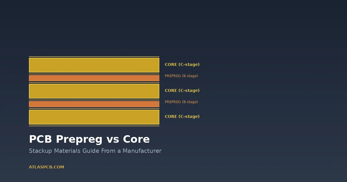
Understanding how prepreg behaves during the lamination press cycle helps engineers appreciate why the same material specification can produce different results depending on processing conditions, panel layout, and adjacent copper patterns. The lamination process subjects prepreg sheets to temperatures between 170°C and 190°C (for standard FR-4 chemistry) while applying pressures of 250-400 PSI over a press cycle lasting 60-120 minutes. During this process, the B-stage resin softens, flows to fill copper pattern gaps on adjacent layers, and then cross-links into a fully cured C-stage thermoset matrix.
The amount of resin flow depends on several interacting factors: the initial resin content of the prepreg, the gelation characteristics of the specific resin system (how quickly viscosity increases with temperature), the lamination pressure profile, and the volume of copper pattern that the resin must fill on adjacent layers. A layer with 30% copper coverage (70% open area that resin must fill) consumes significantly more resin from the adjacent prepreg than a layer with 80% copper coverage (only 20% open area). This differential resin consumption changes the effective dielectric thickness between layers in ways that vary across the board area — regions with dense copper patterns on one layer but sparse patterns on the adjacent layer will see different dielectric thickness than regions where both layers have uniform copper density.
Fabricators compensate for this variability by calculating the expected resin demand from the copper pattern data and selecting prepreg configurations that provide adequate resin volume for the worst-case area of the panel. They may use multiple plies of thin prepreg rather than a single thick ply to provide better thickness uniformity after resin flow. For critical impedance applications, they add copper thieving patterns (non-functional copper fills) to areas with low copper density to equalize resin consumption across the board area. When your design includes both dense BGA regions (high copper density) and sparse routing channels (low copper density) on the same layer, discussing copper balancing strategies with your fabricator during the stackup review stage prevents thickness variations that would otherwise cause systematic impedance differences between different regions of the finished board.
Cost Implications of Prepreg Selection
Material selection decisions cascade through the entire PCB manufacturing cost structure in ways that are not always obvious from the per-sheet price of the prepreg itself. Choosing a thinner glass style to achieve a specific dielectric thickness may require two plies instead of one, doubling the prepreg material cost for that layer while also adding a lamination handling step. Specifying spread-glass prepreg adds material premium but may eliminate the need for diagonal routing strategies that consume additional layers or board area. Understanding these tradeoffs helps engineers make economically informed decisions that achieve their performance requirements without unnecessary cost escalation.
The most common cost-driving prepreg decisions involve the choice between single-ply and multi-ply constructions. Using two sheets of 1080 prepreg instead of one sheet of 2116 to achieve approximately 0.12mm dielectric thickness increases material cost by roughly 30-40% for that specific layer but provides better thickness uniformity (two thin sheets average out individual thickness variations better than one thick sheet) and more consistent Dk behavior (the finer weave of 1080 has less pronounced glass-weave effect). For designs with 4-6 impedance-controlled layers, this choice can add 8-15% to the total board cost — a premium that is easily justified for high-speed applications but unnecessary for standard digital designs operating below 1 GHz.
Spread-glass prepreg typically commands a 15-25% premium over standard-weave material of the same glass style, reflecting the additional mechanical processing required to flatten or open the weave structure. However, this premium applies only to the specific layers where spread-glass is specified — there is no reason to use spread-glass for power plane separation layers or non-impedance-critical dielectric spacing. A practical approach is to specify spread-glass only for the dielectric layers immediately adjacent to high-speed signal traces (the layers that determine their impedance environment) while using standard-weave prepreg for all other layers. This selective specification captures the electrical benefit where it matters while minimizing the total material cost impact.
For designs entering volume production where material cost becomes a significant portion of the per-unit price, working with the fabricator to identify standard prepreg constructions they maintain in inventory avoids minimum-order-quantity premiums and procurement lead time additions. Most established fabricators stock 4-6 prepreg configurations in each glass style across 2-3 resin content levels. Designing your stackup around these standard offerings rather than specifying exotic constructions can reduce material lead time from 3-4 weeks to immediate availability while achieving equivalent electrical performance through minor impedance geometry adjustments (trace width optimization) rather than exotic material specification.
Practical DFM Recommendations
Based on our fabrication experience across thousands of impedance-controlled multilayer designs, the following recommendations help engineers select prepreg configurations that achieve their electrical requirements while maintaining manufacturing margin and cost efficiency.
For designs operating below 5 GHz with standard impedance tolerance of ±10%, use the fabricator’s recommended standard construction. Specify only the total dielectric thickness, material family (standard FR-4, mid-Tg, or high-Tg), and impedance targets. Allow the fabricator flexibility to select glass styles and ply counts based on their standard inventory and process capabilities. This approach minimizes cost and lead time while achieving adequate impedance control for the vast majority of commercial designs.
For designs operating between 5 GHz and 15 GHz with impedance tolerance of ±7%, specify the glass style and number of plies for each impedance-critical dielectric layer. Use 1080 or equivalent fine-weave prepreg for signal-to-reference dielectric layers, and include a note requiring the fabricator to perform impedance simulation with their actual prepreg thickness and Dk data before production. Request impedance test coupon measurement with results reported for each production lot. This level of specification provides meaningful impedance control without over-constraining the fabricator’s process.
For designs operating above 15 GHz or requiring impedance tolerance tighter than ±5%, specify spread-glass prepreg for all signal-layer dielectric spacing, mandate a specific laminate system with documented Dk data at your operating frequency, require a formal stackup review with the fabricator’s process engineer before tooling release, and include insertion loss test coupons in addition to impedance coupons. Consider whether the additional cost of very-low-loss materials (such as Megtron 6, Tachyon 100G, or I-Tera MT40) provides measurable benefit for your specific trace lengths and data rates, or whether a careful stackup design with standard high-speed FR-4 achieves adequate performance at lower cost.
Regardless of operating frequency, always provide your fabricator with copper coverage data for each layer (available as a Gerber analysis report from most EDA tools), specify copper thieving requirements for layers with uneven copper distribution, and request the fabricator’s actual stackup calculation (not a generic template) showing the specific prepreg construction, resin flow assumptions, and resulting impedance predictions for your design. This collaborative approach to prepreg specification — treating it as an engineering discussion rather than a procurement checkbox — consistently produces the most reliable impedance results across production quantities.
Reviewed by AtlasPCB Engineering Team — based on fabrication data from impedance-controlled multilayer production across standard FR-4, high-speed, and RF material systems.
About AtlasPCB — We specialize in complex PCB manufacturing for HDI, RF, and high-reliability applications. Explore our impedance-controlled PCB manufacturing, or get an free engineering DFM review . Every order includes free engineering review. Get your quote.
Reviewed by AtlasPCB Engineering Team — IPC-certified manufacturing specialists with 15+ years of production experience in HDI, RF, and high-reliability PCB fabrication. Content based on factory floor data and real customer design reviews.
Frequently Asked Questions
What is the difference between prepreg glass styles 106, 1080, 2116, and 7628?
How does resin content percentage affect PCB impedance?
Why does glass weave pattern cause impedance variation across a PCB?
When should I specify spread-glass prepreg for my PCB design?
- prepreg
- glass weave
- impedance control
- PCB materials
- DFM
- dielectric constant