· AtlasPCB Engineering · Engineering · 9 min read
PCB Stackup Design Guide: Layer Assignment Strategy for 6-Layer and 8-Layer Impedance-Controlled Boards
A practical layer assignment methodology for impedance-controlled PCB stackups. Covers signal-ground pairing, power plane placement, and the specific prepreg/core combinations that achieve target impedance without custom dielectric orders. Includes downloadable stackup templates for common 6L and 8L configurations.
Quick Answer
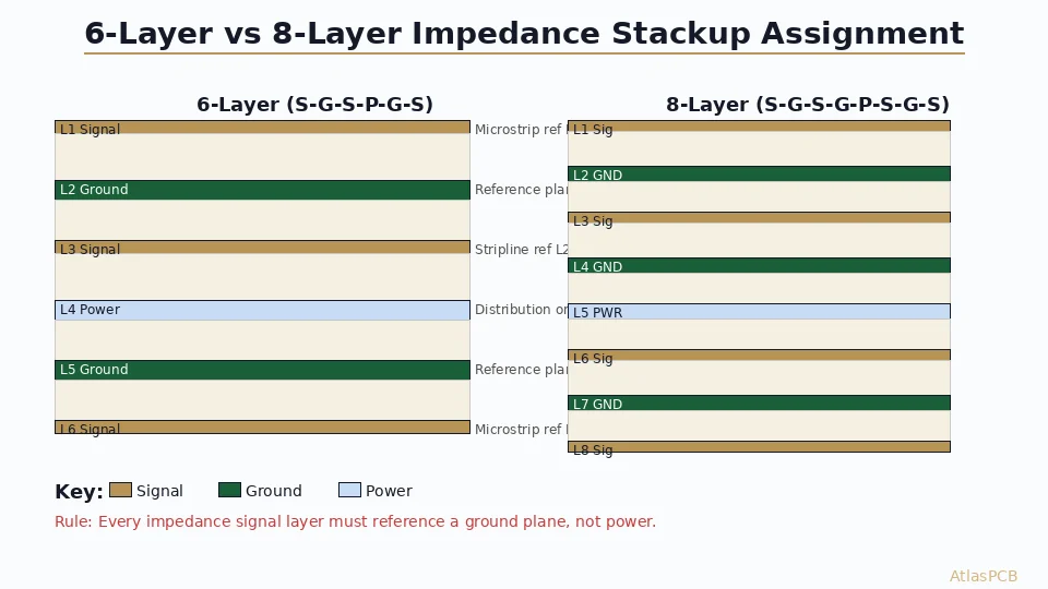
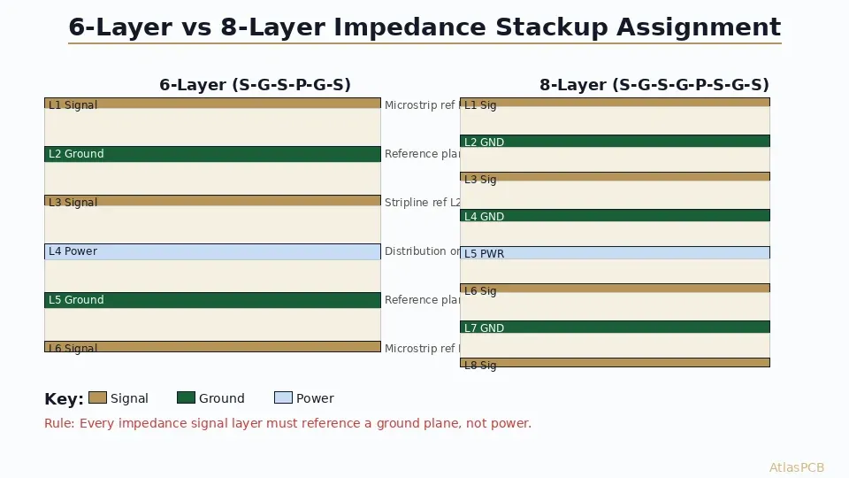
The most common stackup mistake on 6-layer and 8-layer impedance-controlled boards is placing signal layers adjacent to power planes instead of ground planes. Ground-referenced signals achieve 30-40% tighter impedance tolerance because ground planes have continuous copper fill (no splits or vias), while power planes have anti-pads, splits, and decoupling via fields that create localized impedance discontinuities. The optimal 6-layer stackup for mixed impedance is S-G-S-P-G-S; for 8-layer, it is S-G-S-G-P-S-G-S.
Quick Reference: Recommended Stackup Configurations
| Layers | Configuration | Best For | Impedance Performance |
|---|---|---|---|
| 6L | S-G-S-P-G-S | Mixed digital + some RF | +/-7% achievable |
| 6L | S-G-S-G-P-S | High-speed digital, DDR4/5 | +/-5% achievable |
| 8L | S-G-S-G-P-S-G-S | Complex mixed-signal | +/-5% achievable |
| 8L | S-G-S-P-G-S-G-S | High routing density | +/-7% achievable |
Why Layer Assignment Determines Your Impedance Success Rate
The difference between a first-pass impedance success and a costly respin almost always traces back to layer assignment decisions made early in the design, not fabrication errors. In our facility, we review approximately 800 impedance-controlled designs per month, and the single most common DFM issue — accounting for roughly 35% of all engineering queries we raise — is signal layers referenced to power planes instead of ground planes.
This is not a theoretical concern. When we run TDR verification on production panels, boards with power-referenced signal layers consistently show 8-15% impedance variation along the trace length, while ground-referenced signals on the same board achieve 3-5% variation. The physics is straightforward: power planes are not uniform conductors. They have anti-pads around every through-via, voltage domain splits, and variable current density patterns that create localized changes in the effective dielectric geometry seen by the propagating signal.
A properly assigned stackup puts ground planes adjacent to every signal layer that carries impedance-controlled traces. This is non-negotiable for any board targeting better than +/-10% impedance tolerance. The ground plane serves as both the RF return path and the impedance reference — when it has gaps or discontinuities, both signal integrity and impedance control degrade simultaneously.
The 6-Layer Stackup: Getting Three Signal Layers Right
Six-layer boards represent the most common impedance-controlled design we fabricate, and they present the most interesting optimization challenge because you have exactly one fewer plane than ideal. With three signal layers requiring ground references, you need two ground planes — which leaves only one plane for power distribution.
The recommended configuration is S-G-S-P-G-S, read from top to bottom:
Layer 1 (Signal): Microstrip geometry, referenced to L2 ground. This is your highest-impedance-tolerance layer because the reference plane is continuous and the geometry is simple — one conductor over one ground plane with a single dielectric between them. Use this layer for your most critical traces: clock lines, high-speed differential pairs, and RF signals.
Layer 2 (Ground): Continuous ground plane. No splits, no via anti-pad islands (use thermal relief for assembly vias only if required by your process). Every break in this plane degrades L1 and L3 impedance simultaneously.
Layer 3 (Signal): Stripline geometry, referenced to both L2 ground above and L5 ground below. Stripline inherently provides better shielding and slightly tighter impedance tolerance than microstrip because the trace is bounded by ground planes on both sides. However, the dielectric thickness above and below must be matched (symmetric stripline) or explicitly specified as asymmetric.
Layer 4 (Power): Power distribution. This plane carries VCC domains but is NOT used as an impedance reference. Route no impedance-critical traces on L3 that rely on L4 as their return path.
Layer 5 (Ground): Second ground plane. Serves as the lower reference for L3 stripline and the reference for L6 microstrip.
Layer 6 (Signal): Microstrip geometry, referenced to L5 ground. Mirror of L1 from an impedance standpoint.
STACKUP DESIGN SERVICE
Free Stackup Review Before You Route
Send your layer count, impedance targets, and signal speed requirements — our engineers recommend the optimal stackup from standard materials in stock.
Request Stackup Review ›
The 8-Layer Stackup: Full Impedance Control on All Signal Layers
Eight-layer designs give you the luxury of proper ground referencing on every signal layer without compromise. The recommended configuration S-G-S-G-P-S-G-S provides four signal layers, each with dedicated ground reference, plus one power plane for distribution.
| Layer | Function | Thickness (typ.) | Impedance Role |
|---|---|---|---|
| L1 | Signal (microstrip) | 1oz copper | Referenced to L2 GND |
| Core 1 | Dielectric | 4.0mil (Dk 4.2) | L1 impedance control |
| L2 | Ground plane | 0.5oz copper | Reference for L1 and L3 |
| PP 2-3 | Prepreg | 4.7mil (Dk 4.0) | L3 impedance control (upper) |
| L3 | Signal (stripline) | 0.5oz copper | Referenced to L2 GND + L4 GND |
| PP 3-4 | Prepreg | 4.7mil (Dk 4.0) | L3 impedance control (lower) |
| L4 | Ground plane | 0.5oz copper | Reference for L3 and L6 |
| Core 2 | Dielectric | 40mil (total board thickness filler) | Structural |
| L5 | Power plane | 0.5oz copper | Power distribution only |
| PP 5-6 | Prepreg | 4.7mil (Dk 4.0) | L6 impedance control (upper) |
| L6 | Signal (stripline) | 0.5oz copper | Referenced to L5 PWR + L7 GND |
| PP 6-7 | Prepreg | 4.7mil (Dk 4.0) | L6 impedance control (lower) |
| L7 | Ground plane | 0.5oz copper | Reference for L6 and L8 |
| Core 3 | Dielectric | 4.0mil (Dk 4.2) | L8 impedance control |
| L8 | Signal (microstrip) | 1oz copper | Referenced to L7 GND |
Note that L6 is referenced to L5 (power) on one side — this is the compromise in this stackup. If L6 carries impedance-critical signals, ensure the power plane section beneath those traces is a solid unbroken copper flood (single voltage domain, no splits). Alternatively, use the S-G-S-G-G-S-G-S configuration if all four signal layers need ground-only references, sacrificing the dedicated power plane for a power/ground hybrid on one layer.
Prepreg and Core Selection: Using Standard Materials
The most expensive mistake in stackup design is specifying non-standard dielectric thicknesses. Every PCB manufacturer stocks a limited set of core and prepreg materials. Specifying an off-catalog thickness forces special material procurement — adding 2-4 weeks to lead time and 20-40% to material cost.
Our standard inventory for impedance-controlled designs includes:
| Material | Dk (at 1 GHz) | Available Thicknesses | Notes |
|---|---|---|---|
| 1080 prepreg | 4.0-4.2 | 2.7mil, 3.0mil | Single-ply, thin |
| 2116 prepreg | 4.0-4.2 | 4.5mil, 4.7mil | Most common choice |
| 7628 prepreg | 4.2-4.4 | 7.5mil, 8.0mil | Thick, fewer plies needed |
| Core (standard Dk) | 4.2-4.5 | 3.5mil, 4.0mil, 5.0mil, 8.0mil, 10mil, 14mil, 20mil, 31mil, 40mil, 60mil | Wide range |
When designing your stackup, work backward from these available thicknesses. If your impedance calculation requires 4.3mil dielectric, use the 4.5mil prepreg and adjust trace width slightly — do not request custom 4.3mil material. The difference between 4.5mil and 4.3mil prepreg represents approximately 2 ohms on a 50-ohm trace, which is within normal manufacturing tolerance and easily compensated by our etch adjustment process.
Our process engineers routinely optimize impedance by adjusting trace geometry within +/-0.5mil of nominal to hit targets with standard materials. This costs nothing extra and avoids the material procurement penalty entirely.
IMPEDANCE EXPERTISE
We Optimize Your Stackup for Our Standard Materials
Send impedance targets + layer count — we return a DFM-optimized stackup using in-stock materials. No procurement delays, no material upcharges.
Impedance Control Services ›Common DFM Failures in Stackup Design (And How to Avoid Them)
Based on our DFM review data from the past 12 months, here are the stackup-related issues that most frequently cause design respins or impedance failures:
Power plane splits crossing signal traces. When a power plane has voltage domain boundaries, any signal trace that crosses the split loses its reference plane momentarily. The impedance spikes by 15-30% at the crossing point, and the return current must find an alternate path around the split. If your design requires power plane splits, route impedance-controlled traces on layers referenced exclusively to ground planes, not power planes.
Asymmetric stripline without specification. Many designers route signals on internal layers assuming symmetric stripline geometry (equal dielectric above and below). In practice, core and prepreg thicknesses above and below may differ by 1-2mil due to available material combinations. This creates asymmetric stripline with different impedance than calculated. Always specify to your manufacturer whether traces should be calculated as symmetric (equal spacing to both references) or offset stripline (specify which reference is primary).
Insufficient ground via stitching between reference planes. A ground plane provides impedance reference only if it is properly connected to other ground planes and has a low-impedance path for return current. For signals transitioning between layers referenced to different ground planes (e.g., L1 referenced to L2 ground, transitioning via to L3 referenced to L5 ground), stitching vias connecting L2 and L5 ground planes must be placed within lambda/20 of the signal via. At 5 GHz, this means ground via within 1.2mm of the signal via transition.
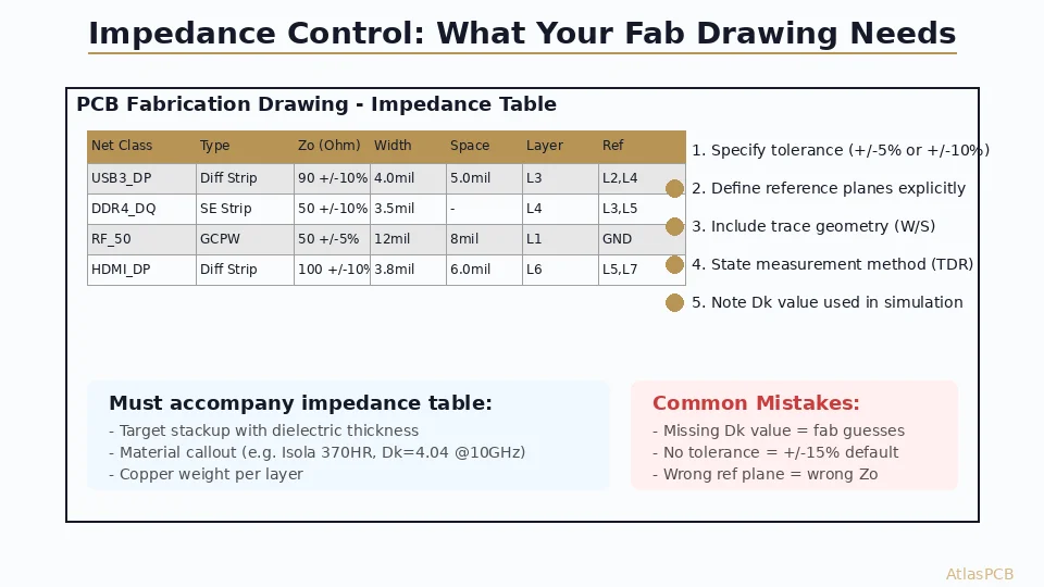
Specifying impedance without identifying reference layers. This is the number one cause of first-article impedance failures in our experience. A note saying “50 ohm +/-10%, all controlled impedance traces” is meaningless without layer-specific reference identification. The correct specification format is: “L1, 50 ohm SE, microstrip, ref L2 GND, 5mil trace target, 1oz Cu.”
Impedance Calculation Verification Before Ordering
Before submitting your design, verify your impedance calculations against your actual stackup dimensions. We recommend using at least two independent calculators to cross-check results — and then request your manufacturer’s simulation as the final authority.
The critical parameters that must be consistent between your calculation and your manufacturer’s are:
- Dk at operating frequency (not the 1 MHz value from material datasheets — Dk drops 5-10% between 1 MHz and 5 GHz for FR-4)
- Dielectric thickness (pressed thickness after lamination, not raw prepreg thickness — prepreg compresses 5-15% during press)
- Copper thickness (plated-up thickness on outer layers is typically 1.0-1.4oz after plating, even when starting with 0.5oz foil)
- Trace cross-section shape (trapezoidal after etching, not rectangular — etch factor changes effective width by 0.5-1.0mil)
In our experience, the discrepancy between designer-calculated impedance and our simulation average is 4-7 ohms on 50-ohm targets, primarily due to Dk value differences and etch factor assumptions. This is why we always recalculate and confirm before fabrication, adjusting trace geometry to hit your target with our actual process parameters.
ATLASPCB
Submit Your Stackup for Free Impedance Simulation
Upload your Gerbers or stackup table. We run 2D field solver simulation, confirm material availability, and return a verified stackup with calculated trace widths — before you commit to production.
Upload and Verify ›
Reviewed by AtlasPCB Engineering Team — 15+ years in advanced PCB fabrication for RF, HDI, and rigid-flex applications.
Related Reading:
About AtlasPCB — We specialize in complex PCB manufacturing for HDI, RF, and high-reliability applications. Explore our HDI PCB manufacturing capabilities, RF and high-frequency PCB services, or get an impedance-controlled PCB manufacturing . Every order includes free engineering review. Get your quote.
Reviewed by AtlasPCB Engineering Team — IPC-certified manufacturing specialists with 15+ years of production experience in HDI, RF, and high-reliability PCB fabrication. Content based on factory floor data and real customer design reviews.
Frequently Asked Questions
What is the best layer stackup for a 6-layer impedance-controlled PCB?
Why does ground reference give better impedance control than power reference?
How do I choose prepreg thickness for target impedance?
Should I specify the exact prepreg and core materials in my stackup?
How does via anti-pad size affect impedance on adjacent traces?
- PCB stackup design guide
- impedance controlled PCB manufacturer
- PCB DFM check
- HDI PCB manufacturer
- RF PCB design and manufacturing