· AtlasPCB Engineering · Engineering · 30 min read
10-Layer PCB Stackup Design: A Manufacturer's Guide to Configurations, Impedance Control, and Cost Optimization
A comprehensive manufacturer's guide to 10-layer PCB stackup design covering three proven configurations with real prepreg and core specifications, impedance calculations, HDI buildup options, common DFM mistakes we see from customers, manufacturing process flow, and detailed cost comparisons against 8-layer and 12-layer alternatives.
Quick Answer
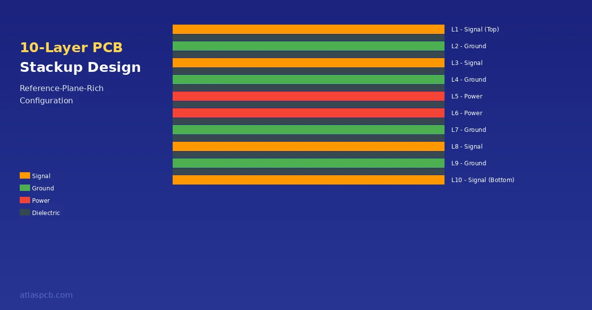
A 10-layer PCB stackup typically uses the configuration SIG/GND/SIG/GND/PWR/GND/SIG/GND/SIG/SIG (reference-plane-rich) or SIG/GND/SIG/PWR/SIG/SIG/PWR/SIG/GND/SIG (routing-dense) with a 1.6mm total thickness. The recommended standard stackup for high-speed designs places four continuous ground planes adjacent to all critical signal layers, using 3.5-4mil prepreg on outer layers for 50-ohm microstrip impedance control. Cost is typically 30-45% more than an equivalent 8-layer board and 25-35% less than a 12-layer board. The primary cost driver beyond layer count is whether HDI (sequential lamination) is required for BGA escape routing.
When an 8-Layer Board Is No Longer Enough
The transition from an 8-layer to a 10-layer PCB stackup represents a deliberate engineering decision that should be driven by quantifiable design constraints rather than a general desire for more routing capacity. In our fabrication facility, approximately 15% of orders above 8 layers are 10-layer designs, and the reasons for stepping up from 8 layers follow consistent patterns that we can articulate with specificity.
The most frequent trigger is high-speed interface density exceeding what four signal layers can support with proper reference plane discipline. An 8-layer board in its optimal configuration provides four signal layers, each with an adjacent ground or power reference. When a design carries three or more independent high-speed interfaces simultaneously — for example, DDR4 at 3200MT/s, PCIe Gen4 x4, USB 3.2 Gen2, and a 10GbE SerDes link — each interface ideally demands its own dedicated routing layer with tight coupling to a continuous ground plane. Attempting to share signal layers between these interfaces forces compromises: either traces from different protocols share a reference plane (risking crosstalk at transition speeds above 5 Gbps) or some signals must route on layers without an immediately adjacent ground reference (degrading impedance control and return-path continuity).
The second trigger involves BGA escape complexity on designs with multiple large-pitch-count packages. A single BGA with 500+ balls at 0.8mm pitch can typically be escaped on an 8-layer board, but when two or three such packages coexist on a board with limited area for fan-out, the routing congestion in the escape regions overwhelms four signal layers. Adding two signal layers through the 10-layer configuration provides the channel capacity to escape these packages without violating 4/4mil minimum trace-and-space rules or resorting to via-in-pad everywhere.
The third scenario is power distribution complexity. Designs requiring four or more distinct voltage domains at moderate-to-high current (greater than 2A per rail) benefit from dedicated power planes rather than routed power traces or localized copper pours. An 8-layer board typically allocates one or two layers to power distribution. A 10-layer stackup can dedicate two full power planes while maintaining four ground planes, creating tightly coupled power-ground pairs that serve as distributed decoupling capacitance across the board.
From a manufacturing perspective, the step from 8 to 10 layers is less disruptive than the step from 6 to 8. Both use the same class of lamination presses, both require the same number of sequential imaging and etching cycles (all layers are processed in parallel during inner-layer fabrication), and both use identical drilling equipment. The primary manufacturing differences are additional material cost (two more copper layers and one more core laminate), slightly longer press cycle times for the thicker book, and marginally tighter registration requirements due to the increased total copper-to-copper stack height.
Not sure if you need 10 layers?
Upload your schematic or preliminary layout and our engineers will analyze your routing density, signal speed requirements, and power distribution needs — then recommend the optimal layer count with a detailed stackup proposal. Free with every quote request.
Get a Free Stackup ReviewThree Proven 10-Layer Stackup Configurations
Every 10-layer PCB design begins with an architectural decision about how to distribute signal, ground, and power layers across the ten available copper planes. The choice fundamentally determines which signals will have ideal reference planes, how power distribution performs at high frequencies, and what manufacturing tolerances the fabricator must hold. After manufacturing tens of thousands of 10-layer panels, we have identified three configurations that address the majority of design requirements. Each makes explicit trade-offs between routing density, signal integrity margin, power distribution quality, and manufacturing yield.
Configuration A: Reference-Plane-Rich (4 Signal / 4 Ground / 2 Power)
This is our recommended configuration for high-speed digital designs where signal integrity takes priority over raw routing capacity. The layer assignments are:
| Layer | Function | Copper Weight | Reference |
|---|---|---|---|
| L1 (Top) | Signal + Components | 1oz (35um) | Microstrip → L2 GND |
| L2 | Continuous Ground | 0.5oz (17um) | — |
| L3 | Signal (High-Speed) | 0.5oz (17um) | Stripline → L2 GND + L4 GND |
| L4 | Continuous Ground | 0.5oz (17um) | — |
| L5 | Power Plane 1 | 1oz (35um) | — |
| L6 | Power Plane 2 | 1oz (35um) | — |
| L7 | Continuous Ground | 0.5oz (17um) | — |
| L8 | Signal (High-Speed) | 0.5oz (17um) | Stripline → L7 GND + L9 GND |
| L9 | Continuous Ground | 0.5oz (17um) | — |
| L10 (Bottom) | Signal + Components | 1oz (35um) | Microstrip → L9 GND |
This arrangement provides the highest signal integrity margin because every signal layer has an immediately adjacent continuous ground plane. Layers 3 and 8 are particularly favored for critical high-speed signals because they sit in a true stripline environment between two ground planes, providing excellent shielding and predictable impedance regardless of adjacent routing activity.
The L5/L6 power plane pair can be configured for multiple voltage domains. In a typical application, L5 carries the primary 3.3V or 1.8V digital core voltage while L6 handles secondary rails (1.2V, 0.9V for DDR VDDQ, or analog supplies). The L4-L5 and L6-L7 spacings create ground-power pairs that provide significant interplane capacitance for mid-frequency decoupling.
The primary limitation is routing capacity: you have only four signal layers (L1, L3, L8, L10), and two of those are outer layers shared with component placement. For designs requiring more than approximately 1,500 routed nets on a standard-density board, this configuration may prove insufficient.
Recommended material construction for 1.6mm total thickness:
| Layer Pair | Material | Thickness (pressed) | Glass Style |
|---|---|---|---|
| L1-L2 | Prepreg | 3.5mil (89um) | 1080 |
| L2-L3 | Core | 6.0mil (152um) | — |
| L3-L4 | Prepreg | 4.0mil (102um) | 1080 |
| L4-L5 | Core | 8.0mil (203um) | — |
| L5-L6 | Prepreg | 8.0mil (203um) | 2116 |
| L6-L7 | Core | 8.0mil (203um) | — |
| L7-L8 | Prepreg | 4.0mil (102um) | 1080 |
| L8-L9 | Core | 6.0mil (152um) | — |
| L9-L10 | Prepreg | 3.5mil (89um) | 1080 |
Configuration B: Balanced (6 Signal / 2 Ground / 2 Power)
This configuration maximizes routing density while maintaining acceptable signal integrity for designs operating below 5 Gbps per lane. It is the most common 10-layer stackup we fabricate for cost-sensitive commercial electronics.
| Layer | Function | Copper Weight | Reference |
|---|---|---|---|
| L1 (Top) | Signal + Components | 1oz (35um) | Microstrip → L2 GND |
| L2 | Continuous Ground | 0.5oz (17um) | — |
| L3 | Signal | 0.5oz (17um) | Stripline → L2 GND + L4 PWR |
| L4 | Power Plane 1 | 0.5oz (17um) | — |
| L5 | Signal | 0.5oz (17um) | Offset stripline → L4 PWR |
| L6 | Signal | 0.5oz (17um) | Offset stripline → L7 PWR |
| L7 | Power Plane 2 | 0.5oz (17um) | — |
| L8 | Signal | 0.5oz (17um) | Stripline → L7 PWR + L9 GND |
| L9 | Continuous Ground | 0.5oz (17um) | — |
| L10 (Bottom) | Signal + Components | 1oz (35um) | Microstrip → L9 GND |
This stackup provides six signal layers, which typically accommodates designs with 2,000-3,000 routed nets on boards up to 200x150mm. The trade-off is that layers 5 and 6 reference power planes rather than ground planes. Power planes are acceptable references for slower signals (below 2.5 Gbps) provided they remain un-split beneath the signal traces and the power plane copper coverage exceeds 80% in the routing region.
The critical design rule when using this configuration: never route high-speed signals on L5 or L6 across power plane splits. The discontinuity in the reference plane creates an impedance discontinuity and forces return current to find an alternate path, generating radiated emissions. Reserve L3 and L8 for the fastest signals (DDR, SerDes, clocks) since they reference ground planes directly, and route slower control signals, address buses, and GPIO on L5 and L6.
Recommended material construction for 1.6mm total thickness:
| Layer Pair | Material | Thickness (pressed) | Glass Style |
|---|---|---|---|
| L1-L2 | Prepreg | 3.5mil (89um) | 1080 |
| L2-L3 | Core | 5.0mil (127um) | — |
| L3-L4 | Prepreg | 4.0mil (102um) | 1080 |
| L4-L5 | Core | 5.0mil (127um) | — |
| L5-L6 | Prepreg | 10.0mil (254um) | 2116x2 |
| L6-L7 | Core | 5.0mil (127um) | — |
| L7-L8 | Prepreg | 4.0mil (102um) | 1080 |
| L8-L9 | Core | 5.0mil (127um) | — |
| L9-L10 | Prepreg | 3.5mil (89um) | 1080 |
Configuration C: Mixed-Signal Optimized (5 Signal / 3 Ground / 2 Power)
This configuration addresses designs that combine sensitive analog circuits with high-speed digital logic — common in data acquisition systems, medical instrumentation, and RF receivers with digital back-ends.
| Layer | Function | Copper Weight | Reference |
|---|---|---|---|
| L1 (Top) | Digital Signal + Components | 1oz (35um) | Microstrip → L2 GND |
| L2 | Continuous Ground (Digital) | 0.5oz (17um) | — |
| L3 | High-Speed Digital Signal | 0.5oz (17um) | Stripline → L2 GND + L4 GND |
| L4 | Continuous Ground (Shared/Split) | 0.5oz (17um) | — |
| L5 | Digital Power | 1oz (35um) | — |
| L6 | Analog Power | 1oz (35um) | — |
| L7 | Continuous Ground (Analog) | 0.5oz (17um) | — |
| L8 | Analog Signal | 0.5oz (17um) | Stripline → L7 GND + L9 GND |
| L9 | Continuous Ground (Analog) | 0.5oz (17um) | — |
| L10 (Bottom) | Signal + Components | 1oz (35um) | Microstrip → L9 GND |
The defining feature of this configuration is the physical separation between digital and analog domains. Digital signals occupy L1 and L3 in the upper half of the stackup, while analog signals route on L8 in the lower half. The L4 ground plane serves as the primary isolation barrier between domains. Where absolutely necessary, L4 may be split into digital and analog ground regions, but we strongly recommend a single continuous ground plane with a defined single-point connection between domains on the PCB layout rather than a physical split in the plane copper.
The L5/L6 power plane pair mirrors this domain separation: digital power on L5 references the L4 ground above it, while analog power on L6 references the L7 ground below it. This creates independent power-ground plane pairs for each domain, minimizing switching noise coupling from digital circuits into sensitive analog measurements.
Impedance Control in 10-Layer Stackups
Impedance control in a 10-layer PCB follows the same physics as any multilayer board, but the additional layers provide more flexibility in selecting the optimal trace-to-reference geometry for each signal class. The key advantage of a 10-layer design is the ability to place critical signals in true stripline environments (sandwiched between two ground planes) while maintaining thin outer dielectrics for tight microstrip impedance control on surface layers.
Microstrip Impedance (Outer Layers L1 and L10)
For outer signal layers referenced to the adjacent ground plane, the impedance is primarily controlled by three parameters: trace width, dielectric thickness to the reference plane, and the effective dielectric constant of the prepreg material.
With our standard 1080 glass style prepreg at 3.5mil pressed thickness (Dk = 4.2 at 1 GHz), the following trace geometries achieve common impedance targets:
| Target Impedance | Trace Width | Dielectric to GND | Copper Weight | Notes |
|---|---|---|---|---|
| 50 ohm SE | 4.3mil | 3.5mil | 1oz outer | Standard single-ended |
| 75 ohm SE | 2.8mil | 3.5mil | 1oz outer | Video/RF signals |
| 90 ohm diff | 3.5mil / 5mil space | 3.5mil | 1oz outer | USB 3.x |
| 100 ohm diff | 3.8mil / 5mil space | 3.5mil | 1oz outer | PCIe, DDR4 |
These values assume solder mask coverage (Dk approximately 3.3) over the traces, which effectively increases coupling and reduces impedance by 2-3 ohms compared to bare copper. Our impedance tolerance for production is plus or minus 10% standard, tightened to plus or minus 7% on request (with coupon verification), or plus or minus 5% for aerospace-grade requirements at additional cost.
Stripline Impedance (Inner Layers L3, L8)
Inner signal layers in a stripline configuration are sandwiched between two reference planes. This geometry provides inherent shielding and more stable impedance because the trace is surrounded by a homogeneous dielectric environment (core material above, prepreg below, or vice versa). However, the dual-reference geometry means the trace couples to both planes, resulting in narrower trace widths for the same target impedance compared to microstrip.
For L3 in Configuration A (between L2 GND and L4 GND with symmetric 4mil/6mil dielectrics above/below):
| Target Impedance | Trace Width | Upper Dielectric | Lower Dielectric | Notes |
|---|---|---|---|---|
| 50 ohm SE | 3.2mil | 4.0mil (prepreg) | 6.0mil (core) | Offset stripline |
| 50 ohm SE | 3.8mil | 5.0mil (sym) | 5.0mil (sym) | Centered stripline |
| 100 ohm diff | 3.2mil / 4mil space | 4.0mil | 6.0mil | DDR4/PCIe |
The asymmetric (offset) stripline is more common in practice because core and prepreg thicknesses rarely match exactly. This asymmetry is not a problem for signal integrity — the impedance calculator accounts for both dielectric thicknesses — but it means the electromagnetic field distribution is slightly uneven, which has minimal practical effect below 10 GHz.
Production Impedance Tolerance Data
From our production database covering over 2,000 verified 10-layer impedance-controlled jobs in the past twelve months, the actual measured impedance distribution shows:
For 50-ohm single-ended targets on outer layers: mean deviation of +0.8 ohms (slight positive bias due to etching copper loss), standard deviation of 1.4 ohms. This means 95% of production boards fall within plus or minus 2.8 ohms of the 50-ohm target — well within the plus or minus 10% (5-ohm) tolerance window.
For 100-ohm differential targets on inner layers: mean deviation of -0.3 ohms, standard deviation of 1.8 ohms. The tighter distribution on differential pairs results from the geometry being less sensitive to individual trace-width variation (both traces in the pair experience the same etching variation, preserving the differential relationship).
These results assume Shengyi S1000-2M material with published Dk of 4.25 at 1 GHz. Actual Dk can vary by plus or minus 0.1 between material lots, which translates to approximately plus or minus 1.2% impedance variation independent of manufacturing process control.
Need precise impedance control for your 10-layer design?
Our engineering team provides free impedance modeling with every 10-layer quote. We will verify your stackup against our actual material Dk data and recommend trace geometries that hit your targets with production margin to spare.
Request Impedance ModelingMaterial Selection for 10-Layer PCBs
Material selection for a 10-layer stackup involves balancing electrical performance requirements against cost, availability, and manufacturing compatibility. The choice affects not only impedance and signal loss but also the fabrication process parameters (lamination temperature and pressure, drill quality, and plating adhesion).
Standard FR-4 Grades
For designs operating below 3 GHz with standard reliability requirements, conventional FR-4 materials provide excellent performance at the lowest cost. The materials we stock for immediate production of 10-layer boards include:
Shengyi S1000-2M (standard Tg 150C) is our highest-volume 10-layer material. It provides Dk of 4.25 at 1 GHz with a dissipation factor (Df) of 0.019. This material is suitable for general-purpose digital designs, consumer electronics, and industrial controls where signal frequencies stay below 3 GHz. The material meets IPC-4101/21 slash sheet requirements and UL 94 V-0 flammability rating.
Shengyi S1000-2 (high-Tg 170C) offers the same electrical properties as S1000-2M but with improved thermal reliability for lead-free assembly processes requiring multiple reflow cycles at 260C peak temperature. We recommend this material for all 10-layer designs undergoing lead-free assembly, particularly when the board will experience three or more thermal cycles during production (top-side reflow, bottom-side reflow, and selective soldering or rework).
ITEQ IT-180A (high-Tg 180C) provides marginally better thermal performance and slightly lower Df (0.016 at 1 GHz) compared to standard FR-4. This material is preferred for automotive and industrial applications requiring AEC-Q100 qualification testing or ISA/IEC 61508 SIL-rated reliability. The 180C glass transition temperature provides additional margin for thermal cycling in under-hood or industrial environments.
Mid-Loss Materials for High-Speed Digital
When signal frequencies exceed 3 GHz or total trace lengths exceed 150mm at data rates above 5 Gbps, standard FR-4 dissipation factor becomes a measurable contributor to insertion loss. Mid-loss laminates bridge the gap between standard FR-4 and expensive PTFE or Rogers materials:
Shengyi S1000-2ME (Dk 4.0, Df 0.010 at 1 GHz) reduces insertion loss by approximately 40% compared to standard FR-4 at the same thickness. The cost premium is approximately 15-20% over standard S1000-2M. This material is suitable for PCIe Gen4, 10GbE, and USB4 applications where trace lengths are moderate (under 200mm).
Panasonic Megtron-4 (Dk 3.8, Df 0.005 at 1 GHz) and the equivalent ITEQ IT-968SE provide significantly reduced loss for designs approaching 10 GHz signaling rates. The cost premium is 40-60% over standard FR-4, but the improved signal margin often eliminates the need for active signal conditioning (retimers or repeaters) that would add component cost and board area.
Hybrid Stackups: Mixing Materials
For cost-sensitive designs where only specific layers carry high-frequency signals, hybrid material stackups place low-loss material selectively while using standard FR-4 for non-critical layers. A common approach in 10-layer designs uses mid-loss prepreg between L2-L3 and L8-L9 (where the highest-speed stripline signals route) while using standard FR-4 cores and prepreg elsewhere.
The manufacturing consideration with hybrid stackups is CTE (coefficient of thermal expansion) mismatch between dissimilar materials. Materials with significantly different resin systems may expand at different rates during lamination and thermal cycling, potentially causing delamination or via barrel cracking at layer transitions. We require that hybrid material combinations pass our internal thermal stress qualification (six cycles from -40C to 150C with microsection verification) before production release.
HDI Variants of 10-Layer Stackups
When standard through-hole vias cannot provide adequate routing density — typically in designs with 0.5mm or finer pitch BGAs or board dimensions too small for the required net count — high-density interconnect (HDI) structures add laser-drilled microvias to the 10-layer stack. Two common HDI build-ups exist for 10-layer applications.
1+8+1 Build (Single Sequential Lamination)
The 1+8+1 configuration adds one microvia layer on top and one on bottom to an 8-layer core structure. The microvias connect only between L1-L2 and L9-L10, providing additional escape routing density on the outer layers without requiring blind vias to deeper layers.
This build is the most cost-effective HDI option for 10-layer boards because it requires only one additional lamination cycle beyond the standard process. The 8-layer core is fabricated first using conventional through-hole processes, then the outer microvia layers are laminated sequentially and laser-drilled.
Microvia specifications for 1+8+1: laser-drilled via diameter of 100um (4mil) pad-to-pad with capture pad diameter of 250um (10mil). Aspect ratio is limited to 0.8:1 for reliable copper plating (maximum dielectric thickness of 80um between connected layers). Microvias can be filled with copper or conductive paste depending on whether via-in-pad design requires a flat surface for component placement.
Cost premium: Approximately 35-50% over a standard (non-HDI) 10-layer board of the same dimensions. The premium covers additional lamination cycles, laser drilling equipment time, and the extra imaging/plating steps for outer layers.
2+6+2 Build (Double Sequential Lamination)
The 2+6+2 configuration provides two microvia layers on each side of a 6-layer core. This allows stacked or staggered microvias spanning from L1 to L3 and from L8 to L10, dramatically increasing routing density in the BGA escape region.
This build is necessary when component density requires via-in-pad with subsequent layer routing that cannot be achieved with a single microvia span. A typical application is a large FPGA with 0.8mm pitch and 1000+ balls, where the inner ball field requires two levels of microvia escape before signals can transition to through-hole vias for routing on internal layers.
The 2+6+2 build requires two sequential lamination cycles per side (four total additional lamination steps beyond a standard process), making it significantly more expensive than the 1+8+1 variant.
Cost premium: Approximately 80-120% over a standard 10-layer board. The doubled sequential lamination cycles, additional laser drilling passes, and tighter registration requirements for stacked via alignment all contribute to the elevated cost. For further details on HDI cost drivers, see our HDI cost comparison guide.
Manufacturing Process for 10-Layer PCBs
Understanding how a 10-layer PCB is physically manufactured helps designers make informed decisions about design rules, tolerances, and cost optimization. The process involves multiple sequential operations that must be precisely coordinated to achieve layer-to-layer alignment within plus or minus 2mil (50um) across all ten copper layers.
Inner Layer Fabrication
The process begins with the fabrication of four double-sided core laminates. Each core is a sheet of FR-4 with copper foil bonded to both sides. For a 10-layer board, the cores typically correspond to layer pairs L2-L3, L4-L5, L6-L7, and L8-L9 (the exact pairing depends on the stackup configuration and the fabricator’s preferred construction method).
Each core undergoes photolithographic imaging: a photoresist film is laminated onto the copper surface, exposed to UV light through a patterned photomask, developed to remove unexposed resist, and then etched in a cupric chloride or alkaline etchant solution to dissolve the unprotected copper. After etching, the remaining resist is stripped, leaving the designed copper pattern on both sides of the core.
For inner layers in a 10-layer board, we typically use 0.5oz (17um) base copper foil, which allows finer trace definition compared to 1oz outer layers. The minimum trace width achievable on inner layers with standard imaging equipment is 3.0mil (75um) for production reliability, though 2.5mil (63um) is possible for prototype quantities with reduced yield expectations.
Lamination (Layer Registration and Bonding)
After all four cores are imaged, etched, and inspected (using automated optical inspection to verify pattern accuracy against the Gerber data), they are assembled into a book with prepreg sheets between each core and on the outer surfaces. Registration pins or optical alignment systems position each core relative to tooling holes with plus or minus 1mil (25um) accuracy.
The assembled book enters a vacuum hydraulic press at 180C (356F) for standard FR-4. The prepreg resin flows under heat and pressure (approximately 300 PSI), filling the inner-layer copper pattern gaps and bonding all layers into a monolithic structure. The press cycle typically runs 90-120 minutes for a 10-layer board, including controlled heat-up and cool-down ramps to prevent thermal stress.
After pressing, the panel is trimmed and inspected for thickness uniformity. Our target is plus or minus 10% of the specified total thickness across the panel area, with local thickness variation (within a single board outline) held to plus or minus 5%.
Drilling
The laminated panel is drilled using CNC drilling machines with carbide micro-drill bits. For a typical 10-layer board with standard through-hole vias, we drill mechanical holes ranging from 0.2mm (8mil) to 6.35mm (250mil) diameter. The critical parameter for 10-layer boards is the drill aspect ratio — the ratio of board thickness to hole diameter.
For a standard 1.6mm thick 10-layer board, the maximum recommended aspect ratio for reliable copper plating is 10:1, which means the minimum via drill size is 0.16mm (6.3mil). In practice, we recommend 0.2mm (8mil) minimum drill for production reliability and 0.15mm (6mil) minimum for prototype quantities. Holes smaller than this require laser drilling (see the HDI section above).
Drill registration to the inner layer patterns relies on X-ray alignment of buried targets. Our standard registration accuracy for 10-layer boards is plus or minus 2mil (50um) from drill center to inner layer pad center, which determines the minimum required annular ring width on inner layers (typically 3.5mil minimum after registration tolerance is applied).
Copper Plating, Outer Layer Imaging, and Finishing
After drilling, the panel undergoes electroless copper deposition (a thin 0.5-1um seed layer) followed by electrolytic copper plating to build the via barrel and surface copper to the final thickness. For 1oz outer copper, the total plated thickness in the via barrel is approximately 25um (1mil), which provides reliable electrical continuity from L1 through all layers to L10.
The outer layers (L1 and L10) are then imaged and etched using a pattern-plating process: photoresist defines the trace pattern, tin-lead or tin is plated over the exposed copper as an etch resist, the photoresist is stripped, and the unprotected copper is etched away. This process achieves finer resolution on outer layers (3.5mil minimum trace for production) than the previous subtractive process because the copper thickness being etched is controlled by plating duration rather than starting foil weight.
Final processing includes solder mask application (liquid photoimageable, LPI), silkscreen legend printing, surface finish application (HASL, ENIG, immersion silver, or OSP depending on requirements), electrical testing (flying probe or fixture-based), and final dimensional routing or V-score panelization.
Manufacturing Timeline
A standard 10-layer PCB production cycle from CAM review completion to shipment-ready boards requires:
| Process Step | Duration | Notes |
|---|---|---|
| Inner layer imaging + etching | 1 day | All 4 cores processed in parallel |
| AOI inspection + oxide treatment | 0.5 day | Copper roughening for adhesion |
| Layup + lamination press | 1 day | Including press cycle + cool-down |
| Drilling | 0.5-1 day | Depends on hole count |
| Copper plating | 1 day | Electroless + electrolytic |
| Outer layer imaging + etching | 1 day | Pattern plate process |
| Solder mask + legend | 1 day | — |
| Surface finish + electrical test | 1 day | — |
| Routing + final inspection | 0.5 day | — |
| Total standard | 7-8 working days | After CAM review completion |
Express service can compress this to 5 working days by overlapping non-dependent steps and prioritizing machine scheduling, at a premium of 30-50% over standard pricing.
Common DFM Mistakes in 10-Layer Designs
After reviewing thousands of 10-layer designs through our engineering DFM check process, we have identified recurring mistakes that cause fabrication issues, increase cost, or degrade electrical performance. These are the errors we flag most frequently during pre-production review.
Mistake 1: Inadequate Annular Ring on Inner Layers
The most common manufacturing issue in 10-layer boards is insufficient annular ring on inner layer pads after drill registration tolerance is applied. With a 10-layer board at 1.6mm thickness, our drill-to-inner-layer registration is plus or minus 2mil. If a designer specifies a via pad of 20mil diameter with a 10mil drill, the nominal annular ring is 5mil per side — but after worst-case registration offset, the minimum ring may be only 3mil, which is below our manufacturing minimum of 3.5mil.
The solution: for 10-layer boards, specify inner layer pads with a minimum diameter of drill size plus 10mil (5mil annular ring per side before registration). This provides adequate margin for the registration tolerance inherent in drilling through nine dielectric layers.
Mistake 2: Routing High-Speed Signals Across Power Plane Splits
In Configuration B (6-signal variant), layers 5 and 6 reference power planes rather than ground planes. Designers frequently split these power planes into multiple voltage islands without considering that signal traces on L5/L6 may cross the split boundaries. When a 5 Gbps signal crosses a plane split, the return current must detour around the gap, creating a large loop antenna that radiates electromagnetic energy and degrades signal quality.
The fix is to either route critical signals only on layers that reference continuous ground planes (L3 and L8 in Config B) or ensure that no signal trace on L5/L6 crosses a split in its reference power plane. This requires close coordination between stackup planning, power domain assignment, and signal routing constraints — ideally established before placement begins.
Mistake 3: Asymmetric Copper Distribution Causing Warpage
A 10-layer stackup must maintain approximate copper symmetry about its center line (between L5 and L6) to prevent bow and twist after lamination. When one side of the board has significantly more copper coverage than the other — for example, a large ground pour on the top half with mostly sparse signal traces on the bottom half — the differential thermal contraction during cool-down from lamination temperature causes the panel to warp.
Our acceptance criterion for bow and twist follows IPC-6012 Class 2: maximum 0.75% for boards less than 2.0mm thick. For a 200mm-long panel, this translates to a maximum deflection of 1.5mm. Boards exceeding this threshold may fail automated assembly placement due to registration errors on warped surfaces.
To prevent this, maintain copper coverage within 15% between corresponding layer pairs (L1 vs L10, L2 vs L9, L3 vs L8, L4 vs L7). If your signal routing creates a significant imbalance, add copper fill (connected to ground where possible, or unconnected thieving patterns) to equalize coverage.
Mistake 4: Via Aspect Ratio Violations
Designers sometimes carry over via specifications from thinner boards without adjusting for the increased total thickness of a 10-layer stack. A via that works perfectly in a 1.0mm 6-layer board (for example, 0.15mm drill = 6.67:1 aspect ratio) becomes marginal or impossible in a 1.6mm 10-layer board (10.67:1 aspect ratio — beyond our standard capability of 10:1).
Before finalizing your via specifications, verify that the minimum drill diameter satisfies the aspect ratio limit for your chosen total board thickness. For our standard process: maximum 10:1 for through-hole vias, 8:1 for reliable IPC Class 3 plating, and 0.8:1 for microvias.
Mistake 5: Missing Stackup Documentation in Fabrication Package
Approximately 20% of 10-layer designs arrive without a formal stackup drawing or with incomplete stackup information. A stackup that specifies “10 layers, 1.6mm, FR-4” without defining layer functions, dielectric thicknesses, impedance requirements, and copper weights forces our engineering team to assume default values — which may not match the designer’s intent.
A complete 10-layer stackup specification should include: layer function assignments (signal/ground/power), target finished thickness, copper weight per layer, controlled impedance requirements with target values and tolerances, material grade or class, and any special requirements (buried capacitance, HDI, mixed materials). Our Gerber files guide includes a stackup template that covers all necessary fields.
Avoid costly DFM issues before they reach production
Every quote request includes a comprehensive DFM review by our engineering team. We check annular rings, aspect ratios, impedance feasibility, copper balance, and 40+ other parameters specific to your layer count — catching problems that cost time and money if found during fabrication.
Submit Design for Free DFM ReviewCost Analysis: 10-Layer vs 8-Layer and 12-Layer
Understanding the cost structure of 10-layer PCBs helps designers make informed decisions about when the additional layers are justified by performance requirements versus when design optimization might allow a lower layer count. The following analysis uses actual production pricing data from our facility for standard specifications (FR-4, 1oz outer / 0.5oz inner copper, HASL finish, standard tolerances).
Direct Cost Comparison
For a reference design of 100x100mm board area at various order quantities:
| Layer Count | 5 pcs (Proto) | 50 pcs (Pilot) | 500 pcs (Production) | 5000 pcs (Volume) |
|---|---|---|---|---|
| 8-layer | $38-48/board | $12-18/board | $4.50-6.50/board | $2.80-3.80/board |
| 10-layer | $52-68/board | $16-24/board | $5.80-8.20/board | $3.50-4.80/board |
| 12-layer | $70-95/board | $22-32/board | $7.50-10.50/board | $4.50-6.20/board |
The 10-layer premium over 8-layer ranges from 30-45% at prototype quantities, narrowing to 25-30% at production volumes. The reduction in relative premium at higher volumes occurs because the fixed cost components (CAM setup, tooling, first-article inspection) are amortized over more boards, leaving material cost (which scales more linearly with layer count) as the dominant factor.
What Drives 10-Layer Cost Beyond Layer Count
Layer count alone is not the primary cost determinant for boards above 8 layers. The following factors can each add 15-50% to the base price and frequently have more impact than the layer count itself:
Minimum trace and space is the single largest cost lever. Moving from 4/4mil minimum to 3/3mil increases cost by 25-40% due to reduced first-pass yield in etching and imaging. If your routing can be completed at 4/4mil or wider on a 10-layer board, you will pay significantly less than a customer requiring 3/3mil on an 8-layer board. In many cases, adding two layers (going from 8 to 10) to relax trace-and-space from 3/3 to 4/4 actually reduces total board cost.
HDI (microvia) requirement adds 35-120% depending on the build complexity (1+8+1 vs 2+6+2). Before specifying HDI, verify whether the BGA escape can be accomplished with standard through-hole vias on a 10-layer board with slightly relaxed via specs (10mil drill, 20mil pad). The additional routing capacity of two extra layers often eliminates the need for HDI.
Material grade affects cost proportionally. Upgrading from standard FR-4 to mid-loss (Megtron-4 equivalent) adds 40-60%, while full RF materials (Rogers 4350B or PTFE) on all layers can triple the material cost. Hybrid stackups that place premium materials only on critical layers offer a 40-50% material cost savings compared to full premium builds.
Controlled impedance with tight tolerance adds 10-20% for standard plus or minus 10% tolerance (due to coupon verification and process control monitoring). Tightening to plus or minus 5% adds another 15-25% because it requires material lot testing, process adjustments per batch, and potentially multiple coupon verifications per panel.
Cost Optimization Strategies
Based on our production experience, the following strategies consistently reduce 10-layer PCB cost without compromising performance:
First, maximize trace-and-space rules. If your design requires 3/3mil on an 8-layer board, consider whether moving to 10 layers allows relaxing to 4/4mil or 5/5mil. The layer count premium (30-45%) is often less than the fine-line premium (25-40%), resulting in a net cost reduction with improved manufacturing yield.
Second, standardize your stackup on commonly available material constructions. Custom core thicknesses and exotic prepreg combinations require special material orders with minimum quantity requirements and extended lead times. Our standard 10-layer material kit (1080 and 2116 prepreg, standard core thicknesses from 4mil to 10mil) ships from stock and avoids material surcharges.
Third, avoid specifying tighter tolerances than your design actually requires. If your signal integrity simulations show adequate margin with plus or minus 10% impedance tolerance, do not specify plus or minus 5%. If your minimum annular ring requirement is met with standard registration, do not request enhanced registration at additional cost.
Fourth, consider panel utilization. Our standard panel size for 10-layer boards is 18x24 inches (457x610mm). Boards that array efficiently on this panel size (filling more than 75% of the available area) receive better per-board pricing than boards with poor panel utilization. If your board outline allows, consider adjusting dimensions by a few millimeters to improve array fit.
Lead Time and Production Considerations
The standard production lead time for a 10-layer PCB at our facility is 10-12 working days from confirmed order (design files accepted, payment received, and engineering questions resolved) to shipment. This timeline includes 1-2 days for CAM engineering review and the 7-8 day fabrication cycle described in the manufacturing process section above.
Factors That Extend Lead Time
Several design choices can push lead time beyond standard:
Non-stock materials require procurement lead time of 5-15 additional working days depending on the material and current supply chain conditions. Standard FR-4 (Shengyi S1000-2M and S1000-2) ships from our warehouse within 24 hours. Mid-loss materials (S1000-2ME) carry 3-5 day lead time. High-frequency laminates (Rogers, Panasonic Megtron-6) may require 10-15 day procurement from authorized distributors.
HDI processing adds 2-4 working days per sequential lamination cycle. A 1+8+1 build adds approximately 3 days; a 2+6+2 build adds 5-7 days.
Controlled impedance with plus or minus 5% tolerance adds 1-2 days for additional process control steps and coupon verification between fabrication stages.
Via-in-pad with copper fill (VIPPO) adds 1-2 days for the additional plating and planarization steps required to achieve flat, solderable pad surfaces over filled vias.
Express Options
For time-critical prototypes, our express service delivers 10-layer boards in 5-7 working days at a premium of 30-50% over standard pricing (dependent on specifications). Emergency service (3-4 working days) is available for standard-specification 10-layer boards at 80-120% premium, subject to manufacturing schedule availability.
The fastest possible 10-layer production we have achieved is 4 working days for a design with standard FR-4, no HDI, no impedance control, and 4/4mil minimum trace/space. Designs with any special processing requirements cannot achieve this timeline regardless of expedite premium.
Choosing Between 8, 10, and 12 Layers: A Decision Framework
The layer count decision should be based on objective, quantifiable criteria rather than intuition or convention. The following framework provides specific thresholds to guide the decision:
Stay at 8 layers when:
- Total routed net count is below 1,200 with standard-density components
- No more than 2 high-speed interfaces requiring dedicated impedance-controlled layers
- BGA packages can be fully escaped with 4 signal layers and standard via rules (10mil drill, 20mil pad)
- Two power planes are sufficient for all voltage distribution requirements
- Board area provides adequate routing space at 4/4mil trace-and-space rules
Move to 10 layers when:
- Net count exceeds 1,200-1,500 with routing congestion at 4/4mil on 8-layer configuration
- Three or more high-speed interfaces each need a dedicated routing layer with continuous ground reference
- BGA packages with 400-700 pins require additional fan-out layers for escape routing
- Three or more power planes are needed for complex PDN requirements
- Mixed-signal design requires physical isolation between analog and digital domains
- Adding two layers allows relaxing trace/space from 3/3mil to 4/4mil (net cost neutral or negative)
Move to 12 layers when:
- Net count exceeds 2,500-3,000 and routing cannot complete on 10-layer at acceptable trace/space rules
- BGA packages with 800+ pins and 0.65mm or finer pitch require additional routing layers
- More than 4 high-speed interfaces each need isolated routing layers
- Five or more power planes are required for complex multi-rail PDN
- The design requires 6+ controlled-impedance signal layers with adjacent continuous references
This framework applies to standard (non-HDI) through-hole designs. HDI can shift these thresholds significantly by providing additional routing density without adding layers, though at increased cost per layer. For designs near the 8-to-10 or 10-to-12 boundary, we recommend submitting your preliminary design for our free stackup review — our engineers can often identify routing strategies or HDI options that optimize the layer count decision.
Connecting to Your Next Design
A well-designed 10-layer stackup provides the foundation for complex high-speed and mixed-signal designs without the cost and complexity of higher layer counts. The key principles to carry forward are: prioritize reference plane continuity over routing density, select your stackup configuration based on signal integrity requirements rather than defaulting to the most common arrangement, and engage your fabricator early in the stackup planning process rather than after layout completion.
For further reading on related topics, see our guides on 6-layer PCB stackup design for simpler designs that may not require 10 layers, 16-layer PCB stackup design for more complex requirements, controlled impedance PCB design calculations for detailed impedance modeling methodology, and multilayer PCB cost comparison for pricing context across different layer counts.
Ready to start your 10-layer PCB project?
Upload your Gerber files or stackup requirements for an instant quote with free DFM review and impedance modeling. Our engineering team reviews every 10-layer design for manufacturability, copper balance, and impedance feasibility before production — ensuring first-article success.
Get Your 10-Layer PCB QuoteReviewed by AtlasPCB Engineering Team
About AtlasPCB — We specialize in complex PCB manufacturing for HDI, RF, and high-reliability applications. Explore our HDI PCB manufacturing capabilities, impedance-controlled PCB manufacturing, or get an Megtron 6 & 7 low-loss PCB manufacturing . Every order includes free engineering review. Get your quote.
Reviewed by AtlasPCB Engineering Team — IPC-certified manufacturing specialists with 15+ years of production experience in HDI, RF, and high-reliability PCB fabrication. Content based on factory floor data and real customer design reviews.
Frequently Asked Questions
What is the best 10-layer PCB stackup for high-speed design?
How much does a 10-layer PCB cost compared to 8-layer?
When should I use 10 layers instead of 8 layers?
What is the standard thickness for a 10-layer PCB?
- 10-layer PCB
- PCB stackup
- stackup design
- impedance control
- multilayer PCB
- PCB manufacturing
- DFM
- HDI PCB
- high-speed PCB