· AtlasPCB Engineering · Engineering · 27 min read
6-Layer PCB Stackup Design: Configurations, Material Specs, Impedance Calculations, and Cost Analysis
A manufacturer's guide to 6-layer PCB stackup design covering three proven configurations with real prepreg and core specifications, worked impedance calculations, HDI buildup options, DFM rules, fab drawing templates, and detailed cost comparisons against 4-layer and 8-layer alternatives.
Quick Answer
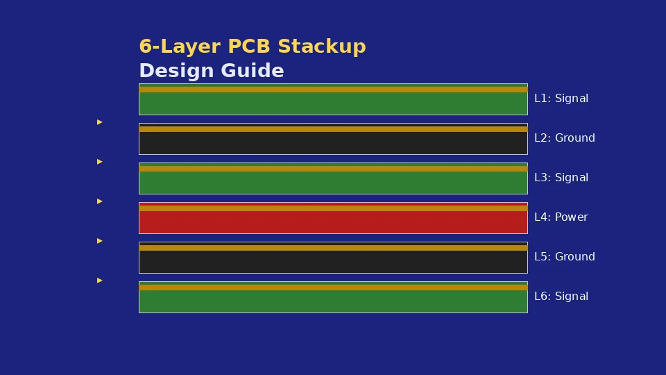
A 6-layer PCB stackup typically uses the configuration SIG/GND/SIG/PWR/GND/SIG with a 1.6mm total thickness. The recommended standard stackup uses 4mil prepreg (1080 glass style) on outer layers for tight impedance control, 47mil core between L2-L3, 4mil prepreg between L3-L4, and 47mil core between L4-L5. For 50-ohm single-ended microstrip on outer layers: use 4.5mil trace width over 4mil dielectric (Dk=4.2). For 100-ohm differential: 4mil traces with 5mil spacing. Cost is typically 1.5-2x a comparable 4-layer board due to additional lamination cycles, imaging steps, and tighter registration requirements.
When a 4-Layer Board Is No Longer Enough
The decision to move from a 4-layer to a 6-layer PCB stackup should be driven by specific, verifiable design constraints rather than a vague sense that more layers equate to better performance. In our fabrication facility, we process thousands of designs annually, and the patterns that trigger a 6-layer requirement are remarkably consistent across different product categories and engineering teams.
The most common trigger is routing density driven by high-pin-count components. A BGA package with 200 or more pins requires escape routing that simply cannot be completed on two signal layers without violating minimum trace width and spacing rules. The arithmetic is straightforward: a 0.8mm-pitch BGA with a 15x15 ball array has 225 signals that need to fan out to the board perimeter. With standard 4/4mil trace/space design rules, you can escape approximately 2-3 rows per signal layer through the ball field channels. On a 4-layer board with two signal layers, that gives you access to 4-6 rows of balls before you run out of routing channels. The remaining inner balls have no path to the outside world without a via transition to an additional signal layer.
The second trigger involves high-speed interface isolation. When a single board carries multiple high-speed protocols simultaneously, such as DDR4 memory running at 2400MT/s alongside a PCIe Gen3 x4 link and a USB 3.1 port, each interface demands its own impedance-controlled routing layer with an adjacent solid ground reference. On a 4-layer board, you have only two surfaces available for controlled-impedance routing, and both reference the same ground plane on layer 2. Crosstalk between interfaces sharing a reference plane becomes a significant signal integrity concern at these data rates. A 6-layer stackup provides the additional layer separation needed to isolate these interfaces without compromising their return path continuity.
Power distribution complexity represents the third common trigger. Designs requiring more than three distinct voltage rails at moderate current levels benefit enormously from a dedicated internal power layer. On a 4-layer board, power distribution typically shares space with signal routing on layers 1 and 4, using wide traces or copper pours that consume valuable routing real estate. A 6-layer stackup moves power distribution to a dedicated internal plane, freeing surface layers entirely for signal routing and component placement. This is particularly valuable for mixed-signal designs where analog power rails must be physically separated from digital supplies to prevent switching noise coupling.
Need help deciding between 4 and 6 layers?
Upload your design files and our engineering team will review your stackup requirements, recommend the optimal layer count, and provide impedance modeling — free with every quote.
Get a Free Stackup ReviewThree Proven 6-Layer Stackup Configurations
Every 6-layer PCB design begins with a fundamental architectural decision: how to distribute signal, ground, and power layers across the six available copper layers. After fabricating hundreds of thousands of 6-layer panels, we have identified three configurations that cover the vast majority of design requirements. Each makes different trade-offs between routing density, signal integrity, power distribution, and manufacturing cost.
Configuration A: SIG/GND/SIG/PWR/GND/SIG (Recommended Standard)
This is the configuration we recommend for most applications and the one we stock standard prepreg and core materials to support at the shortest lead times. The layer assignments are:
Layer 1 (Top): Signal routing and components. Microstrip transmission line referenced to L2 ground plane. Layer 2: Continuous ground plane. Primary reference for L1 and L3 signals. Layer 3: Internal signal routing. Offset stripline referenced to L2 (ground) above and L4 (power) below. Layer 4: Power plane. May be split into multiple voltage islands. Layer 5: Continuous ground plane. Reference for L6 signals and return path for L4 power. Layer 6 (Bottom): Signal routing and components. Microstrip referenced to L5 ground plane.
This configuration excels because it provides three critical advantages simultaneously. First, both outer signal layers have an immediately adjacent ground plane for tight impedance control with thin dielectrics. Second, the L4/L5 power-ground pair creates significant interplane capacitance that serves as a distributed decoupling network across the entire board area. Third, the internal signal layer (L3) is sandwiched between two reference planes, creating a shielded stripline environment for the most sensitive traces such as clock signals, high-speed serial data, and analog signal paths.
The primary limitation is that you have only three signal layers available (L1, L3, L6), with one of those (L3) being an internal layer without component access. For designs with extremely high routing density, this may not provide sufficient channel capacity.
Configuration B: SIG/GND/SIG/SIG/GND/SIG (Maximum Routing Density)
Layer 1 (Top): Signal routing and components. Microstrip referenced to L2. Layer 2: Continuous ground plane. Reference for L1 and L3. Layer 3: Internal signal routing. Offset stripline referenced to L2 above, loosely coupled to L4. Layer 4: Internal signal routing. Offset stripline referenced to L5 below, loosely coupled to L3. Layer 5: Continuous ground plane. Reference for L4 and L6. Layer 6 (Bottom): Signal routing and components. Microstrip referenced to L5.
This configuration maximizes routing density by providing four full signal layers. It is appropriate for designs with very high net counts but moderate signal speeds, where routing completion is the primary challenge rather than signal integrity or power distribution. Industrial control boards with dozens of connectors, LED driver boards with hundreds of individual LED connections, and test fixtures with high pin-count are typical applications.
The critical weakness is the absence of a dedicated power plane. Power must be routed as wide traces or copper pours on signal layers, which consumes routing space and provides inferior decoupling compared to a continuous plane pair. Additionally, the two internal signal layers (L3 and L4) share a thick dielectric between them without an intervening reference plane, creating a broadside coupling path that can produce crosstalk between layers. We strongly recommend orthogonal routing (horizontal on L3, vertical on L4) to mitigate this coupling.
Configuration C: SIG/GND/PWR/SIG/GND/SIG (Enhanced EMC)
Layer 1 (Top): Signal routing and components. Microstrip referenced to L2. Layer 2: Continuous ground plane. Reference for L1 and shield above L3. Layer 3: Power plane. Tightly coupled to L2 ground for maximum interplane capacitance. Layer 4: Internal signal routing. Stripline between L3 (power) and L5 (ground). Layer 5: Continuous ground plane. Reference for L4 and L6. Layer 6 (Bottom): Signal routing and components. Microstrip referenced to L5.
This configuration sacrifices one signal layer to create an extremely effective power distribution and shielding structure. The L2/L3 ground-power pair with thin dielectric between them creates substantial interplane capacitance — at 4mil spacing with standard FR-4, this plane pair provides approximately 150pF per square centimeter of decoupling capacitance distributed uniformly across the board. This dramatically reduces the number of discrete decoupling capacitors needed and provides lower-inductance power delivery at high frequencies where discrete capacitors become ineffective.
The trade-off is clear: only three signal layers remain (L1, L4, L6), with L4 being the premium routing layer due to its position between two reference planes. This configuration is ideal for designs where EMC compliance is critical and routing density is manageable — such as RF front-end modules, precision measurement equipment, and automotive electronics that must pass stringent radiated emissions testing.
Material Selection and Real Stackup Dimensions
The most common frustration engineers express when researching PCB stackup design is the gap between conceptual diagrams showing “thin prepreg” and “thick core” and the actual material specifications needed to complete a fabrication drawing. This section bridges that gap with the specific materials and dimensions we use in production for standard 6-layer constructions.
Standard 1.6mm 6-Layer Stackup (Configuration A)
The following stackup represents our recommended standard construction for a 1.6mm (63mil) finished thickness 6-layer board. All dimensions are nominal cured thicknesses:
L1 Copper: 1oz (1.4mil / 35um) — outer layer, plated to approximately 1.8mil after pattern plating. Prepreg L1-L2: 1x1080 glass style, 2.8mil (71um) cured thickness, resin content 65%, Dk = 4.2 at 1GHz. L2 Copper: 1oz (1.4mil / 35um) — ground plane. Core L2-L3: FR-4 core, 18.6mil (0.47mm), Dk = 4.4 at 1GHz. L3 Copper: 1oz (1.4mil / 35um) — internal signal. Prepreg L3-L4: 1x1080 glass style, 2.8mil (71um) cured thickness, resin content 65%, Dk = 4.2 at 1GHz. L4 Copper: 1oz (1.4mil / 35um) — power plane. Core L4-L5: FR-4 core, 18.6mil (0.47mm), Dk = 4.4 at 1GHz. L5 Copper: 1oz (1.4mil / 35um) — ground plane. Prepreg L5-L6: 1x1080 glass style, 2.8mil (71um) cured thickness, resin content 65%, Dk = 4.2 at 1GHz. L6 Copper: 1oz (1.4mil / 35um) — outer layer, plated to approximately 1.8mil after pattern plating.
Total stackup: 1.4 + 2.8 + 1.4 + 18.6 + 1.4 + 2.8 + 1.4 + 18.6 + 1.4 + 2.8 + 1.4 = 54.2mil copper and dielectric, plus solder mask both sides (approximately 0.8mil each) and surface finish (ENIG adds approximately 0.2mil). Final board thickness: approximately 56mil nominal, which falls within the standard 1.6mm plus or minus 10% tolerance window (57.6-70.4mil or 1.44-1.76mm).
For designs requiring wider impedance control margins or different trace geometries, we also stock 2116 glass style prepreg (4.6mil cured thickness, Dk = 4.25) and 7628 glass style prepreg (7.1mil cured thickness, Dk = 4.5). The 2116 prepreg allows wider trace widths for 50-ohm impedance on outer layers, which simplifies etching and improves yield at the cost of slightly reduced routing density.
Material Grade Options
For standard commercial applications (operating temperature below 130 degrees Celsius, no lead-free assembly requirements beyond standard SAC305), we recommend Shengyi S1000-2M or ITEQ IT-180A laminate. Both materials provide a glass transition temperature of 170-180 degrees Celsius, adequate thermal reliability for 6x reflow cycles, and well-characterized dielectric properties for impedance modeling.
For applications requiring enhanced thermal performance — such as automotive under-hood electronics, power conversion modules, or boards undergoing multiple rework cycles — we recommend upgrading to Shengyi S1000-2 (Tg = 180 degrees Celsius, Td = 360 degrees Celsius) or Isola 370HR (Tg = 180 degrees Celsius, Td = 340 degrees Celsius). These materials provide superior z-axis expansion control during thermal cycling, reducing the risk of barrel crack failures in plated through-holes that see repeated thermal excursions.
For designs operating above 3GHz where dielectric loss becomes a significant concern, standard FR-4 may no longer provide acceptable insertion loss performance. In these cases, mid-loss materials such as Shengyi S1000-2ME (Df = 0.010 at 10GHz) or Panasonic Megtron 4 (Df = 0.005 at 10GHz) offer substantial signal integrity improvement while maintaining compatibility with standard FR-4 processing equipment. The cost premium for mid-loss materials is typically 30-50% over standard FR-4 at the laminate level, which translates to approximately 15-25% at the finished board level since material cost represents only a portion of total fabrication cost.
Impedance Calculations for Standard 6-Layer Configurations
Impedance control is the primary reason engineers choose specific dielectric thicknesses and trace geometries in their stackup design. The following worked examples use our standard 1.6mm stackup dimensions and demonstrate the calculations for the most commonly specified impedance values.
Outer Layer Microstrip: 50-Ohm Single-Ended
For the standard stackup with 1080 prepreg (h = 2.8mil, Dk = 4.2 at 1GHz) between L1 and L2:
Using the IPC-2141 microstrip approximation: Z0 = (87 / sqrt(Dk + 1.41)) x ln(5.98h / (0.8w + t))
Where h = 2.8mil (dielectric height), w = trace width (unknown), t = 1.4mil (copper thickness after etching, before plating).
Solving for Z0 = 50 ohms: 50 = (87 / sqrt(4.2 + 1.41)) x ln(5.98 x 2.8 / (0.8w + 1.4)) 50 = (87 / 2.369) x ln(16.744 / (0.8w + 1.4)) 50 = 36.72 x ln(16.744 / (0.8w + 1.4))
ln(16.744 / (0.8w + 1.4)) = 1.362 16.744 / (0.8w + 1.4) = 3.904 0.8w + 1.4 = 4.289 w = 3.61mil
In practice, we specify 3.5mil trace width for 50-ohm single-ended microstrip on this stackup, which yields calculated impedance of approximately 51 ohms — well within the standard plus or minus 10% tolerance. Note that this narrow trace width requires laser direct imaging (LDI) for reliable patterning; our standard process capability supports 3/3mil trace/space with LDI.
Outer Layer Microstrip: 100-Ohm Differential
For differential pairs on the outer layer with the same 1080 prepreg stackup:
Using the edge-coupled microstrip differential impedance formula: Zdiff = 2 x Z0 x (1 - 0.48 x exp(-0.96 x s/h))
Where Z0 is the single-ended impedance of each trace, s = trace spacing (edge-to-edge), and h = dielectric height.
For 4.0mil trace width (Z0 approximately 48 ohms) with 5.0mil spacing: Zdiff = 2 x 48 x (1 - 0.48 x exp(-0.96 x 5.0/2.8)) Zdiff = 96 x (1 - 0.48 x exp(-1.714)) Zdiff = 96 x (1 - 0.48 x 0.180) Zdiff = 96 x (1 - 0.0864) Zdiff = 96 x 0.914 Zdiff = 87.7 ohms
This is below our 100-ohm target. Increasing spacing to 7.0mil: Zdiff = 2 x 48 x (1 - 0.48 x exp(-0.96 x 7.0/2.8)) Zdiff = 96 x (1 - 0.48 x exp(-2.4)) Zdiff = 96 x (1 - 0.48 x 0.0907) Zdiff = 96 x (1 - 0.0436) Zdiff = 96 x 0.956 Zdiff = 91.8 ohms
Still below target. For reliable 100-ohm differential on this thin stackup, we recommend either: reducing trace width to 3.5mil (increasing Z0 to approximately 51 ohms) with 5mil spacing, giving Zdiff approximately 93 ohms; or using 2116 prepreg (h = 4.6mil) which allows 4.0mil traces with 5.5mil spacing to achieve 100 ohms. Our impedance modeling team runs full-wave 2D field solver simulations (not simplified formulas) for production impedance calculations, accounting for trapezoidal trace cross-sections, solder mask effects, and actual copper roughness profiles.
Internal Stripline: 50-Ohm Single-Ended (Layer 3)
For signals on L3, referenced to L2 (ground) above and L4 (power) below:
The dielectric distances are asymmetric: 18.6mil core above (to L2) and 2.8mil prepreg below (to L4). This creates an offset stripline configuration where the trace is much closer to the lower reference plane.
For offset stripline impedance: Z0 = (60 / sqrt(Dk)) x ln(4 x b / (0.67 x pi x (0.8w + t)))
Where b = total distance between reference planes = 18.6 + 1.4 (L3 copper) + 2.8 = 22.8mil. However, for offset stripline, the effective calculation uses the distances to each plane individually.
A practical result from our field solver: with the standard stackup dimensions, a 5.0mil trace width on L3 yields approximately 50 ohms single-ended impedance. The asymmetry means the trace couples more strongly to L4 (power plane) than to L2 (ground plane), which is acceptable provided L4 is a solid plane or the trace does not cross any splits in the power plane.
Impedance modeling included with every order
Our engineers run full 2D field solver simulations for your specific stackup and provide a detailed impedance report with recommended trace widths before fabrication begins. No additional charge.
Request Impedance Modeling6-Layer HDI Option: The 1+4+1 Buildup
Not all 6-layer PCBs are created equal in terms of manufacturing complexity. A standard 6-layer through-hole board uses plated through-holes (PTH) that traverse all six layers. A 6-layer HDI board with a 1+4+1 buildup introduces blind microvias on the outer layers, connecting L1 to L2 and L5 to L6 without penetrating the entire board. This architectural difference has profound implications for routing density, component packaging support, and cost.
The 1+4+1 designation means: one buildup layer on top (L1, connected to L2 by blind laser-drilled microvias), four core layers in the middle (L2-L5, connected by standard mechanical through-holes), and one buildup layer on the bottom (L6, connected to L5 by blind microvias). The central four layers are fabricated as a standard 4-layer board first, then the outer buildup layers are laminated and laser-drilled in a sequential process.
When to Choose HDI 6-Layer Over Standard PTH 6-Layer
The decision point is component density rather than electrical performance. Standard PTH 6-layer boards can achieve equivalent signal integrity to HDI versions — the impedance and crosstalk characteristics are determined by dielectric geometry, not via type. However, PTH boards waste significant routing space because every through-hole via creates a no-go zone on all six layers simultaneously. A single 0.3mm drill with 0.5mm pad (minimum annular ring of 0.1mm) blocks a 20mil diameter circle on every layer, regardless of whether the connection needs to traverse all layers.
HDI microvias solve this problem by confining each via connection to only the layers involved. A blind via from L1 to L2 consumes pad space only on those two layers, leaving L3 through L6 completely free for routing. For a BGA with 0.5mm pitch requiring fanout to inner layers, HDI construction can reduce the required board area by 20-40% compared to an equivalent PTH design, or alternatively, allow the same board size to accommodate additional components.
The cost premium for 1+4+1 HDI construction over standard PTH 6-layer is typically 30-50% for prototype quantities and 25-40% at production volumes. This premium reflects the sequential lamination process (two press cycles instead of one), laser drilling equipment time, and additional imaging registration steps. For designs where the HDI construction enables a smaller board size, the net cost impact may be minimal or even favorable because the reduced board area offsets the per-square-inch cost increase.
HDI Design Rules Specific to 6-Layer 1+4+1
Our standard HDI process capability for 6-layer 1+4+1 construction:
Blind microvia diameter: 0.1mm (4mil) minimum laser-drilled hole, 0.25mm (10mil) capture pad. Microvia aspect ratio: Maximum 0.8:1 (depth to diameter ratio). For 2.8mil prepreg plus 1.4mil copper, total depth is approximately 4.2mil — well within the 0.8:1 limit for a 4mil via. Via-in-pad: Supported with resin fill and copper cap for BGA applications. Registration tolerance: Plus or minus 2mil layer-to-layer for blind via alignment (tighter than PTH due to sequential processing with optical alignment). Minimum trace/space on buildup layers: 3/3mil (75/75um) with LDI imaging.
These capabilities enable direct pad connection for 0.4mm-pitch BGAs without dog-bone fanout, which is the primary driver for HDI adoption in mobile, wearable, and high-density computing applications.
Design for Manufacturing: 6-Layer Specific DFM Rules
Six-layer fabrication introduces manufacturing considerations that do not exist in simpler 2-layer or 4-layer constructions. Understanding these constraints during the design phase prevents costly respins and yield issues during production.
Layer-to-Layer Registration
The fundamental challenge of multilayer PCB fabrication is aligning all internal layers within acceptable tolerances during lamination. Each additional layer pair introduces cumulative registration error. For a 6-layer board, the worst-case misalignment between any two non-adjacent layers (such as L1 to L5) includes contributions from three separate registration steps: the inner layer core imaging, the lamination pin registration, and the outer layer drilling registration.
Our standard registration capability for 6-layer construction is plus or minus 3mil (75um) layer-to-layer. This means an annular ring that appears as 5mil on the artwork will have a worst-case minimum of 2mil (5 minus 3) in production. Since IPC-6012 Class 2 requires minimum 1mil annular ring after all processing, your design annular ring should be at minimum 4mil to guarantee compliance. We recommend 5mil minimum annular ring for all 6-layer designs to provide comfortable production margin.
For pad-to-trace clearances on internal layers, the same registration budget applies. A clearance of 6mil on artwork becomes a worst-case 3mil in production after registration tolerance consumption. Designs with less than 8mil internal clearances on 6-layer boards carry increased risk of shorting defects during lamination registration drift.
Copper Balance Across All Six Layers
Copper density uniformity across layers is more critical in 6-layer boards than 4-layer boards because the additional layers create more opportunities for asymmetric stress during lamination and thermal cycling. The ideal target is copper density within plus or minus 15% across all layers. Ground and power planes naturally have high copper density (typically 75-95% after thermal relief pads and clearances), while signal layers may have only 20-40% copper density depending on routing density.
The solution is copper thieving (dummy fill) on signal layers to bring their density closer to the plane layers. Our standard DFM review automatically checks for copper imbalance and recommends thieving patterns. For the pattern to be effective, thieving copper should be grounded (connected to the ground net) rather than floating, as floating copper can create unpredictable antenna effects and capacitive coupling to adjacent traces.
Minimum Via-to-Via Spacing
Through-hole vias in 6-layer boards have longer barrels than in 4-layer boards, which means the plating chemistry must deposit copper deeper into the hole. The consequence for design rules is that via-to-via spacing must account for the larger hole preparation zone used in wet processing. Our minimum via-to-via spacing for 6-layer construction is 8mil edge-to-edge (measured between finished hole walls), which translates to approximately 12mil center-to-center for standard 0.3mm drill vias with 0.5mm pads.
Designs that violate this spacing risk insufficient plating adhesion between adjacent vias due to chemical entrapment during the electroless copper seed layer process. The symptom is intermittent opens that pass electrical testing at room temperature but fail during thermal cycling as the weak plating bond fractures under z-axis expansion stress.
How to Specify Your 6-Layer Stackup on a Fab Drawing
A complete stackup specification on your fabrication drawing eliminates ambiguity and prevents the manufacturer from making assumptions that may not align with your design intent. We review hundreds of stackup specifications monthly, and the most common source of manufacturing delays is incomplete or ambiguous stackup documentation.
Required Stackup Information
Your fabrication drawing or separate stackup document should include all of the following:
Layer identification and function: Clearly label each layer (L1 through L6) with its function — signal, ground plane, power plane, or split plane. If a power layer contains multiple voltage islands, identify each island and its net name.
Copper weight per layer: Specify starting copper weight (before processing). Standard options are 0.5oz (18um), 1oz (35um), and 2oz (70um). If different layers require different weights, specify each individually.
Dielectric material and thickness: For each dielectric layer, specify the material type (prepreg or core), glass style (1080, 2116, 7628), number of sheets if stacking multiple prepreg plies, and target cured thickness. Include the material grade (standard Tg, mid-Tg, high-Tg, halogen-free) by reference to a specific laminate system or by specification of required Tg and Td values.
Total board thickness: Specify target finished thickness with tolerance. Standard is 1.6mm plus or minus 10% (1.44-1.76mm).
Impedance requirements: For each controlled-impedance structure, specify: the layers involved, target impedance value, tolerance (standard is plus or minus 10%), trace width, and trace spacing (for differential pairs). Reference the dielectric layer used for the calculation.
Example Fab Note Stackup Specification
The following text block represents what should appear on your fabrication drawing or in an accompanying specification document:
STACKUP SPECIFICATION - 6 LAYER, 1.6mm Nominal
Layer 1: Signal (1oz Cu), Microstrip 50-ohm SE (w=3.5mil), 100-ohm Diff (w=4.0mil, s=5.5mil) Prepreg: 1x1080, 2.8mil nominal, Dk=4.2 at 1GHz (Shengyi S1000-2M or equivalent) Layer 2: Ground Plane (1oz Cu) - continuous, no splits Core: 18.6mil FR-4, Dk=4.4 at 1GHz Layer 3: Signal (1oz Cu), Stripline 50-ohm SE (w=5.0mil) Prepreg: 1x1080, 2.8mil nominal, Dk=4.2 at 1GHz Layer 4: Power Plane (1oz Cu) - split: 3.3V, 1.8V, 1.2V (see power layer drawing) Core: 18.6mil FR-4, Dk=4.4 at 1GHz Layer 5: Ground Plane (1oz Cu) - continuous, no splits Prepreg: 1x1080, 2.8mil nominal, Dk=4.2 at 1GHz Layer 6: Signal (1oz Cu), Microstrip 50-ohm SE (w=3.5mil), 100-ohm Diff (w=4.0mil, s=5.5mil)
Finished thickness: 1.6mm +/- 10% Material: FR-4, Tg >= 170C, CTI >= 175V, UL94-V0, halogen-free preferred Impedance tolerance: +/- 10%, TDR coupon verification required
This level of specification allows the manufacturer to order materials, configure lamination programs, and calculate process parameters without design clarification delays. Omitting any of these details typically adds 1-2 days to the engineering review stage as we contact you for clarification.
Cost Analysis: 6-Layer vs 4-Layer vs 8-Layer
Understanding the cost structure of multilayer PCBs helps engineers make informed decisions about layer count and avoid both over-engineering (paying for unnecessary layers) and under-engineering (forcing designs onto too few layers and paying for EMC failures or routing respins later).
Cost Multipliers by Layer Count
Based on our current production pricing for standard FR-4 boards at typical prototype and production quantities:
4-Layer PCB: Baseline reference (1.0x). Standard construction with two signal layers, one ground plane, one power plane. Single lamination press cycle, two inner layer imaging steps.
6-Layer PCB: 1.5-2.0x of 4-layer cost. Additional expense comes from: second lamination press cycle (core plus buildup construction), two additional inner layer imaging and etching steps, tighter registration requirements consuming more panel edge space (reducing utilization), longer overall process flow (typically 2 additional production days), and marginally higher material cost for additional prepreg and copper foil.
8-Layer PCB: 2.0-2.8x of 4-layer cost (or approximately 1.3-1.5x of 6-layer cost). Adds another lamination cycle beyond 6-layer, plus additional imaging steps. However, the incremental cost from 6 to 8 layers is smaller than the jump from 4 to 6 layers because the manufacturing infrastructure (registration systems, multilayer press capacity) is already engaged.
What Drives 6-Layer Cost Variation
Within the 1.5-2.0x range for 6-layer boards, several factors determine where a specific design falls:
Board size: Larger boards consume more material per unit but may allow better panel utilization (more boards per manufacturing panel). The sweet spot for cost efficiency is boards between 50x50mm and 150x150mm.
Copper weight: Standard 1oz on all layers is included in base pricing. Heavy copper (2oz or 3oz) on any layer adds 15-25% due to longer etching times, different chemistry requirements, and reduced imaging resolution.
Minimum feature sizes: Designs with 4/4mil or finer trace/space require LDI imaging instead of conventional exposure, adding approximately 10-15% to cost. Standard 5/5mil designs can use conventional imaging on most layers.
Impedance control: Controlled impedance adds approximately 5-10% for TDR coupon fabrication, measurement documentation, and potentially tighter process controls. Multiple impedance structures on different layers do not significantly increase cost beyond the base controlled-impedance charge.
Surface finish: ENIG adds approximately 10-15% over HASL for 6-layer boards. OSP is cost-neutral. Immersion silver and immersion tin fall between HASL and ENIG.
Quantity effects: Setup costs (tooling, imaging film or LDI programming, lamination fixturing) are amortized across the order quantity. At 5-10 prototype boards, setup dominates and cost per board is high. At 100+ boards, material and processing time dominate. At 1000+ boards, material costs become the primary factor and the 6-layer premium over 4-layer compresses toward the lower end of the range (approximately 1.5x).
Cost Optimization Strategies for 6-Layer Designs
Several design decisions can reduce 6-layer fabrication cost without compromising electrical performance:
Use standard dielectric thicknesses that match stock prepreg and core materials. Non-standard thicknesses require special material procurement with minimum order quantities and longer lead times.
Minimize the number of unique drill sizes. Each drill tool change adds cycle time. Standardize on 0.2mm, 0.25mm, 0.3mm, and 0.4mm as your primary via drill sizes and avoid specifying unusual diameters unless electrically necessary.
Design board outlines as simple rectangles or shapes that tile efficiently on manufacturing panels. Internal cutouts, complex outlines, and non-rectangular shapes reduce panel utilization and increase routing time.
Specify the minimum surface finish that meets your assembly and reliability requirements. HASL (lead-free) is lowest cost and perfectly adequate for most applications without fine-pitch components (above 0.5mm pitch).
Get an instant 6-layer PCB quote
Upload your Gerber files for automated pricing, or describe your requirements for a custom stackup recommendation. Standard 6-layer prototypes ship in 5-7 business days.
Get Your 6-Layer QuoteThermal Management Considerations for 6-Layer Stackups
The additional copper layers in a 6-layer board provide significantly more thermal mass and lateral heat spreading capability compared to 4-layer construction. Two continuous ground planes (L2 and L5) act as large-area copper heat spreaders, distributing heat from localized hot spots across the full board area. This passive thermal management capability reduces the temperature rise at component junctions without requiring additional heatsinking in many applications.
For designs with concentrated heat sources such as power regulators, motor drivers, or high-current LED drivers, the internal planes can be leveraged as thermal conduits by placing thermal vias directly under the heat source. A thermal via array connecting the component thermal pad on L1 through all layers to exposed copper on L6 creates a low-resistance thermal path through the board thickness. Our recommended thermal via pattern uses 0.3mm drill vias on a 1.0mm grid (approximately 100 vias per square centimeter), which provides thermal resistance of approximately 20 degrees Celsius per watt through the board thickness — a four-fold improvement over the same board area without thermal vias.
The interaction between thermal via arrays and signal routing requires careful planning during stackup configuration. Thermal via arrays create no-go zones for routing on all internal layers. In Configuration A (SIG/GND/SIG/PWR/GND/SIG), thermal vias passing through L3 (the internal signal layer) block routing channels. If your design has both high thermal dissipation requirements and high routing density on L3, consider Configuration C (SIG/GND/PWR/SIG/GND/SIG), which places the internal signal layer (L4) farther from the top surface where most power components are mounted, potentially reducing thermal via interference with signal routing.
Manufacturing Process Overview: How 6-Layer Boards Are Built
Understanding the fabrication sequence helps engineers appreciate why certain design rules exist and where manufacturing risks concentrate. A standard 6-layer PTH board follows this production sequence:
The process begins with inner layer core fabrication. Two double-sided cores are produced: Core 1 (carrying L2 and L3 copper patterns) and Core 2 (carrying L4 and L5 copper patterns). Each core goes through photoresist lamination, UV exposure through a phototool or LDI, chemical development, acid copper etching to remove unwanted copper, and resist stripping. The resulting patterns are inspected by automated optical inspection (AOI) to verify trace geometry and detect shorts or opens. Inner layer defects caught here are inexpensive to scrap; defects missed here become yield-killing failures in the finished board.
After inner layer inspection, the cores receive oxide or oxide-alternative surface treatment to promote adhesion between copper surfaces and the prepreg resin during lamination. The treated cores are then stacked in precise registration with prepreg sheets and outer copper foils. The complete stack — copper foil, prepreg, Core 1, prepreg, Core 2, prepreg, copper foil — is placed in a hydraulic press at approximately 180 degrees Celsius and 300 PSI for 60-90 minutes. The prepreg resin melts, flows to fill all gaps, and crosslinks into a rigid thermoset matrix that permanently bonds all layers together.
Once laminated, the panel is a solid slab with no electrical connections between layers. Mechanical drilling creates through-holes at all via and component hole locations. The holes are cleaned (desmear process to remove resin from internal copper pads), activated with palladium catalyst, and plated with electroless copper to create a conductive seed layer on all hole walls. Panel electroplating then builds copper thickness on all surfaces and hole walls simultaneously to approximately 1mil (25um) minimum in holes, meeting IPC-6012 reliability requirements.
The outer layer pattern is created through photoresist imaging and pattern plating (copper followed by tin or tin-lead etch resist), then the panel is etched to remove background copper while protecting the circuit pattern. After stripping the etch resist, solder mask is applied, imaged, and cured, followed by surface finish application (ENIG, HASL, OSP, etc.), legend printing, and final routing to individual board outlines.
The entire process for a standard 6-layer board requires 12-15 major processing steps and typically takes 5-7 working days from material preparation to shipping. Rush processing can compress this to 3-4 days by prioritizing the job through each department, though this premium service carries additional charges.
Reviewed by AtlasPCB Engineering Team
This article reflects manufacturing data and process capabilities from our Shenzhen and Huizhou production facilities, verified against current material specifications from our laminate suppliers (Shengyi Technology and ITEQ Corporation) as of August 2026. Impedance calculation examples are verified against Polar Si9000 field solver results. All cost data reflects current market pricing and may vary based on material availability and order-specific requirements.
About AtlasPCB — We specialize in complex PCB manufacturing for HDI, RF, and high-reliability applications. Explore our HDI PCB manufacturing capabilities, impedance-controlled PCB manufacturing, or get an free engineering DFM review . Every order includes free engineering review. Get your quote.
Reviewed by AtlasPCB Engineering Team — IPC-certified manufacturing specialists with 15+ years of production experience in HDI, RF, and high-reliability PCB fabrication. Content based on factory floor data and real customer design reviews.
Frequently Asked Questions
What is the best 6-layer PCB stackup configuration?
How much does a 6-layer PCB cost compared to 4-layer?
What materials are used in a standard 6-layer PCB stackup?
When should I use 6 layers instead of 4 layers?
- 6-layer PCB
- PCB stackup
- stackup design
- impedance control
- multilayer PCB
- PCB manufacturing
- DFM
- HDI PCB