· AtlasPCB Engineering · Engineering · 11 min read
HDI PCB DFM Checklist: 8 Microvia and Stackup Errors That Cause 90% of Fabrication Rejections
Most HDI PCB fabrication rejections trace back to the same 8 design errors. This checklist covers microvia aspect ratios, annular ring requirements, stacked via fill specifications, and asymmetric buildup issues — with exact thresholds your manufacturer uses to accept or reject your design.
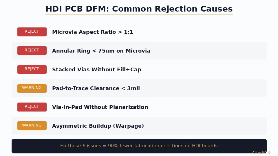
Quick Answer
The 8 most common HDI PCB DFM rejections are: microvia aspect ratio exceeding 1:1, annular ring below 75um on laser vias, stacked microvias without copper fill and cap plating, pad-to-trace clearance below 75um, via-in-pad without planarization specification, asymmetric buildup causing warpage, buried via span exceeding 3 layers, and insufficient anti-pad clearance on ground planes. Fixing these issues before submission eliminates 90% of fab rejections and prevents costly respins.
The 30-Second Checklist
Before submitting your HDI design to any manufacturer, verify these 8 parameters. Each one represents a hard fabrication limit — violating any single item means your board either gets rejected outright or manufactured with unacceptable yield.
| # | DFM Check | Threshold | Consequence of Violation |
|---|---|---|---|
| 1 | Microvia aspect ratio | Max 1:1 (0.8:1 recommended) | Plating void, open circuit |
| 2 | Annular ring on laser via | Min 75um (100um preferred) | Breakout, short to adjacent net |
| 3 | Stacked via fill specification | Must specify IPC-4761 Type VII | Thermal cycling failure at 500 cycles |
| 4 | Pad-to-trace clearance | Min 75um | Short circuit, yield loss >10% |
| 5 | Via-in-pad planarization | Must specify +/-10um flatness | Solder void, tombstoning |
| 6 | Buildup symmetry | Mirror around core | Warpage >0.75%, assembly failure |
| 7 | Buried via span | Max 3 layers | Registration failure, open |
| 8 | Anti-pad on ground plane | Min 200um to via wall | Capacitive coupling, impedance shift |
Error 1: Microvia Aspect Ratio Exceeding 1:1
This is the single most common rejection reason for HDI designs coming from engineers new to microvia technology. The confusion arises because through-hole vias can achieve 10:1 or even 16:1 aspect ratios with mechanical drilling, leading designers to assume similar depth-to-width ratios work for laser vias.
Laser-drilled microvias use CO2 or UV-YAG lasers to ablate the dielectric material. The resulting hole has a tapered profile (not cylindrical like mechanical drills) — wider at the top, narrower at the bottom. Electroless copper plating must then coat this tapered hole uniformly. When the aspect ratio exceeds 1:1, the plating chemistry cannot reliably reach the bottom of the via. The result is thin or absent copper at the via bottom, creating a high-resistance connection that passes electrical test at room temperature but fails under thermal cycling or current load.
In our production environment, we set the manufacturing limit at 0.85:1 to provide process margin. For a standard 65um (2.5 mil) laser-drilled microvia, this means maximum dielectric thickness of approximately 55um. If your stackup requires thicker dielectrics between layers, increase the via diameter accordingly or use a two-stage drilling approach (larger CO2 pre-drill followed by UV-YAG finishing).
How to fix it: If your stackup puts 100um dielectric between adjacent layers, your microvia diameter must be at least 100um (finished hole). Design to 125um for production margin. If routing density prevents 125um vias, reduce the prepreg thickness or switch to a thinner core.
FREE DFM REVIEW WITH EVERY QUOTE
Catch HDI Errors Before Fabrication
Our CAM engineers flag microvia aspect ratio, annular ring, and stackup issues within 24 hours of Gerber submission. No additional charge.
Upload Gerber Files ›
Error 2: Annular Ring Below 75um on Laser Vias
Annular ring — the copper pad area surrounding the drilled hole — is more critical on HDI microvias than on through-hole vias because registration tolerances stack differently in sequential lamination. Each lamination cycle introduces additional layer-to-layer alignment error, typically +/-25um per cycle on modern equipment and +/-50um on older presses.
For a 1+N+1 buildup (single sequential lamination), the registration tolerance between the microvia pad on L1 and its landing pad on L2 is approximately +/-25um. With 75um annular ring design, you have 50um remaining margin after registration — adequate for production. But for a 3+N+3 buildup where the outermost microvia must align through three sequential lamination cycles, the cumulative registration error can reach +/-50-75um. In this case, 75um annular ring leaves almost zero margin, and yield drops dramatically.
The practical rule: for 1+N+1 and 2+N+2 buildups, design to 100um annular ring and accept 75um minimum. For 3+N+3 and above, design to 125um annular ring minimum. If your routing density cannot accommodate larger pads, discuss with your fabricator about their specific registration capability before finalizing the design.
What we see in production: About 30% of incoming HDI designs have at least one via with annular ring below 75um after accounting for our registration tolerance. We flag these in DFM review rather than attempting to fabricate — a breakout on a single via can create an intermittent open that passes in-circuit test but fails in the field.
Error 3: Stacked Microvias Without Copper Fill and Cap
This error kills boards in the field rather than in fabrication — making it particularly dangerous. The board may pass all electrical tests at the factory, ship to the customer, get assembled, and then fail after thermal cycling in operation.
When microvias are stacked (via on top of via), the lower via must be completely filled with conductive copper and planarized flat before the upper via is drilled into it. Without fill, the upper laser drill hits the void inside the lower via, creating an unpredictable connection. Even if the hole walls make contact, the air pocket trapped inside expands during reflow soldering (260C peak) and can crack the via barrel.
IPC-4761 defines via fill types. For stacked microvias, you must specify Type VII (conductive copper fill with cap plating, planarized to +/-10um). Simply stating “filled vias” in your fab drawing is insufficient — some shops interpret this as non-conductive epoxy fill, which does NOT support stacked via construction.
Cost impact: Copper-fill via processing adds one electroplating step plus mechanical planarization (surface grinding) per sequential lamination cycle. Budget approximately 15-20% cost premium over unfilled vias. However, this is non-negotiable for stacked construction — there is no cheaper alternative that works reliably.
Error 4: Pad-to-Trace Clearance Below 75um
High-density routing on HDI layers often pushes designers to minimize clearances. The temptation is real — going from 100um to 50um clearance can free up enough space to avoid adding another routing layer (saving significant cost). But the yield mathematics do not favor this trade-off.
At 75um clearance, standard HDI fabrication achieves 98%+ yield for shorts/opens. At 50um, yield drops to 90-95% depending on the fabricator’s equipment vintage and process control. At 35um, yield falls below 85% on most equipment. The cost of 5-15% yield loss (scrapped panels, repeat runs, delayed delivery) typically exceeds the cost of the additional layer you were trying to avoid.
The trace-to-via clearance is particularly critical because via pads have annular ring variation from registration, while traces have width variation from etching. These two tolerances compound at the minimum clearance point. A trace with +0.5mil etch variation adjacent to a via pad with -25um registration shift can close a 75um gap to 25um — still likely acceptable — but a 50um designed gap would close to zero, creating a dead short.
Our recommendation: Design to 100um clearance everywhere possible. Use 75um only where necessary for BGA breakout. Below 75um requires explicit discussion with your manufacturer about their capability and expected yield impact.
HDI MANUFACTURING CAPABILITY
3/3mil Trace/Space, 0.075mm Laser Drill
Up to 5+N+5 buildup with stacked microvias, via-in-pad, and per-panel yield tracking. Engineering-grade HDI fabrication.
Error 5: Via-in-Pad Without Planarization Specification
Via-in-pad technology places microvias directly in component pads — essential for fine-pitch BGA breakout (0.4mm pitch and below) where escape routing through dog-bone vias is geometrically impossible. The error occurs not in using via-in-pad itself, but in failing to specify the fill and planarization requirements clearly in the fabrication drawing.
An unfilled or improperly filled via-in-pad creates a solder void during reflow. Molten solder wicks down into the open via, leaving a crater on the pad surface. For BGA joints, this void can consume 30-60% of the solder volume, dramatically reducing joint reliability and causing opens during thermal cycling. For QFN center ground pads, the solder wicking creates uneven thermal contact that increases junction temperature.
The correct specification reads: “Via-in-pad, IPC-4761 Type VII, conductive copper fill, planarized to +/-10um from adjacent copper surface.” Some designers specify +/-25um, which is acceptable for larger-pitch BGAs (0.8mm+) but marginal for 0.4mm pitch where solder paste volume is already minimal.
Cost note: Via-in-pad with copper fill adds approximately $2-5/board at prototype quantities (5-10 pieces). At production volumes (1000+), it adds $0.30-0.80/board. This is trivial compared to the cost of BGA rework or field returns from solder voiding.
Error 6: Asymmetric Buildup Construction
PCB warpage during fabrication is governed by the balance of forces across the board’s cross-section. When the stackup is asymmetric — either in copper distribution, dielectric thickness, or number of sequential lamination cycles — differential thermal expansion during lamination and cooling creates a permanent bow or twist.
IPC-6012 Class 2 allows maximum 0.75% warpage (7.5mm per meter). Class 3 allows 0.5%. For BGA assembly, practical warpage limits are even tighter — most SMT lines require boards flatter than 0.3-0.5% for reliable paste printing and placement accuracy. An asymmetric HDI buildup can easily exceed these limits.
Common asymmetric designs that cause warpage:
- 3+N+1 buildup (three sequential laminations on top, one on bottom)
- Heavy copper on one side only (e.g., power plane on L1, no matching plane on L-bottom)
- Different prepreg types on top versus bottom (e.g., high-resin content on top, standard on bottom)
The solution is straightforward: mirror the construction around the core. If your design requires 3 sequential build-up layers on the component side, add 3 on the solder side as well — even if those layers carry minimal routing. The copper fill on “unused” layers should match the copper density of their mirror counterpart. This adds layer cost but prevents assembly yield loss from warpage.
Error 7: Buried Via Span Exceeding 3 Layers
Buried vias (mechanically drilled vias internal to the board that do not reach either surface) become increasingly difficult to fabricate reliably as their span increases. A buried via spanning 2 layers (e.g., L3-L4) is straightforward — it is drilled and plated on a sub-lamination before final layup. A via spanning 3 layers (L2-L4) requires careful processing but remains manufacturable. Beyond 3 layers, the aspect ratio of the buried hole becomes problematic for plating uniformity, and the registration between multiple sub-laminations degrades alignment.
For HDI designs that need deep internal interconnect, the preferred approach is a combination of short-span buried vias and stacked microvias. For example, instead of a single buried via from L2 to L6, use a buried via from L3-L5 (2-span) and connect to L2 and L6 via microvias from the sequential lamination layers. This approach is more complex in design but far more manufacturable and reliable.
Error 8: Insufficient Anti-Pad Clearance on Ground Planes
When a signal via passes through a ground or power plane layer, the anti-pad (clearance hole in the plane copper) must be large enough to prevent capacitive coupling that shifts impedance, but small enough to maintain return current path integrity. For HDI boards with via pitch down to 0.5mm, anti-pad sizing becomes a balancing act.
The minimum anti-pad clearance (from via barrel wall to plane copper edge) is 200um for reliable fabrication. Below 200um, drill wander and registration tolerance can bring the via wall dangerously close to the plane copper, creating potential shorts or degraded insulation resistance that fails under humidity or voltage stress.
For signal integrity, the anti-pad diameter also affects the via’s characteristic impedance. A typical 0.25mm drill with 200um clearance creates a 0.65mm anti-pad. At high speed (above 10 Gbps), the anti-pad’s capacitive discontinuity must be modeled — but from a DFM perspective, just ensure the 200um minimum is maintained on all internal planes.
ENGINEERING SUPPORT
Not Sure About Your HDI Stackup?
Our process engineers review HDI designs for all 8 DFM criteria before quoting. We flag issues and suggest solutions — so your first build works.
Submit Design for Review ›DFM Quick-Reference: Design Rules by HDI Buildup Level
| Parameter | 1+N+1 | 2+N+2 | 3+N+3 | 4+N+4 / Any-Layer |
|---|---|---|---|---|
| Min microvia diameter | 100um | 100um | 75um | 75um |
| Min annular ring | 75um | 100um | 100um | 125um |
| Min trace/space | 75/75um | 75/75um | 50/50um | 50/50um |
| Registration tolerance | +/-25um | +/-35um | +/-50um | +/-50um |
| Min pad-to-trace clearance | 75um | 75um | 75um | 100um |
| Anti-pad clearance | 200um | 200um | 200um | 225um |
| Recommended copper fill | Optional | Required for stack | Required | Required |
Note: These are manufacturing limits, not design targets. Design 20-30% above these values wherever routing density allows, and only approach limits where geometrically forced (BGA breakout, tight pitch connectors).
ATLASPCB
HDI PCB Manufacturing: Up to 5+N+5 Buildup
75um laser drill, 3/3mil trace/space, stacked microvias with copper fill. Engineering-grade quality with per-panel inspection.
Get HDI PCB Quote ›
Reviewed by AtlasPCB Engineering Team — 15+ years in advanced PCB fabrication for RF, HDI, and rigid-flex applications.
Related Reading:
About AtlasPCB — We specialize in complex PCB manufacturing for HDI, RF, and high-reliability applications. Explore our HDI PCB manufacturing capabilities, multilayer PCB fabrication up to 30 layers, or get an free engineering DFM review . Every order includes free engineering review. Get your quote.
Reviewed by AtlasPCB Engineering Team — IPC-certified manufacturing specialists with 15+ years of production experience in HDI, RF, and high-reliability PCB fabrication. Content based on factory floor data and real customer design reviews.
Frequently Asked Questions
What is the maximum aspect ratio for a microvia?
What minimum annular ring is required for HDI microvias?
Why does my HDI PCB warp during fabrication?
Do stacked microvias require copper fill?
What is the minimum trace-to-via clearance for HDI?
- PCB DFM check
- HDI PCB manufacturer
- microvia design
- PCB stackup design guide
- HDI fabrication