· AtlasPCB Engineering · Engineering · 23 min read
8-Layer PCB Stackup Design: Configurations, Impedance Control, Via Planning, and Cost Optimization
A manufacturer's guide to 8-layer PCB stackup design covering three proven configurations with real material specifications, impedance calculations, via structure planning, common fabrication mistakes, and detailed cost analysis comparing 6-layer and 10-layer alternatives.
Quick Answer
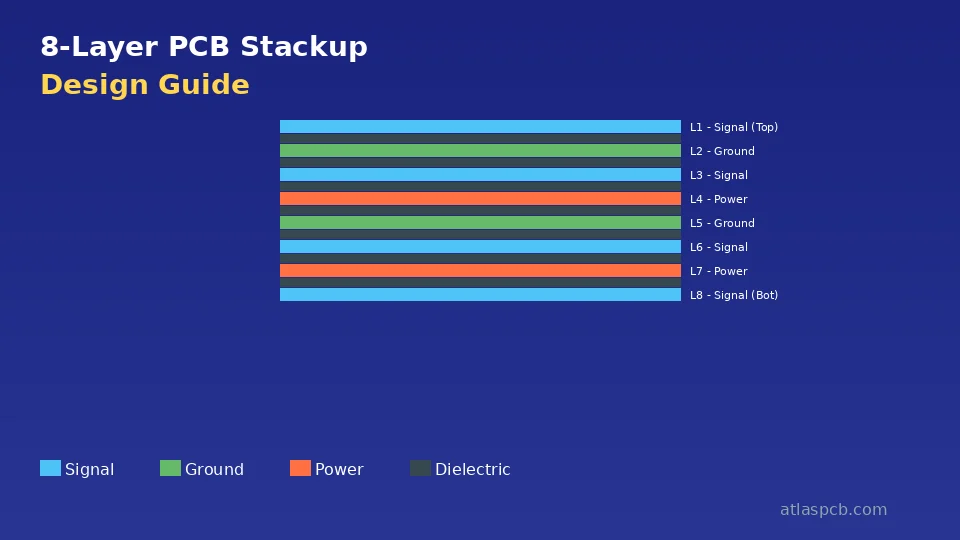
An 8-layer PCB stackup typically uses the configuration SIG/GND/SIG/PWR/GND/SIG/PWR/SIG with 1.6mm total thickness. The recommended standard stackup pairs every signal layer with an adjacent reference plane for optimal impedance control and EMI performance. Construction uses three FR-4 cores (typically 0.2mm each) bonded with four prepreg layers. 8-layer boards cost approximately 30-50% more than equivalent 6-layer designs due to additional lamination cycles and tighter registration requirements. The primary reasons to choose 8 layers over 6 are BGA escape routing requiring four signal layers, multiple high-speed interfaces needing dedicated reference planes, or power distribution requiring two separate power planes for voltage isolation.
When You Need an 8-Layer PCB — and When You Do Not
The transition from a 6-layer to an 8-layer PCB stackup represents a meaningful step in both design capability and manufacturing cost. Unlike the jump from 4 to 6 layers, which often resolves fundamental routing impossibilities, the move to 8 layers is typically driven by a combination of factors that collectively exceed what 6 layers can accommodate without compromising performance. Understanding these thresholds prevents both under-engineering (which leads to signal integrity failures) and over-engineering (which wastes budget on unnecessary layer count).
In our fabrication facility, approximately 35% of the 8-layer boards we manufacture could theoretically function as 6-layer designs with modified routing strategies. The engineers who chose 8 layers did so for valid reasons — reduced design time, better margins on impedance targets, or future-proofing for a revision that adds interfaces — but cost-sensitive projects benefit from rigorous evaluation before committing to the additional layers.
The clearest indicator that 8 layers are necessary is the simultaneous presence of multiple high-speed interfaces that each require dedicated impedance-controlled routing layers with adjacent solid reference planes. A design carrying DDR4 memory (requiring tight length matching on a single layer), a PCIe Gen4 x4 link (requiring differential pair isolation), USB 3.2 (requiring impedance-controlled differential pairs), and Gigabit Ethernet (requiring transformer-side routing) genuinely needs four signal layers with proper reference plane adjacency. Attempting to share signal layers between these interfaces on a 6-layer board forces compromises in return path continuity that degrade signal integrity at multi-gigabit data rates.
The second common trigger is BGA component density. When a design includes two or more fine-pitch BGAs (0.65mm pitch or below) with pin counts exceeding 300, the escape routing challenge becomes severe. Each BGA requires multiple via transitions to route inner ball rows to the board perimeter, and with only two internal signal layers available on a 6-layer board, routing congestion beneath the package creates minimum spacing violations that cannot be resolved without adding layers.
Power distribution complexity provides the third justification. Designs requiring complete electrical isolation between power domains — such as separate analog and digital supplies, or multiple switching regulator outputs that must not share return paths — benefit from having two dedicated power planes rather than relying on split planes. A split power plane on a single layer creates discontinuities in the return current path that can generate EMI and degrade signal integrity for traces crossing the split boundary.
When 8 Layers Is Over-Engineering
Not every complex design requires 8 layers. We frequently review customer designs where 6 layers with HDI (blind/buried vias) would achieve the same routing density at lower total cost, particularly for boards smaller than 50mm x 50mm where the per-panel cost of HDI processing is offset by the panel utilization improvement from fewer layers. Similarly, designs with moderate signal speeds (under 5 Gbps) and single BGA components rarely benefit from the additional layers. The cost premium of 30-50% over a 6-layer board should purchase measurable performance improvement, not simply engineering convenience.
Not sure whether you need 6 or 8 layers?
Send us your schematic and BOM. Our engineering team will analyze your routing density, signal speed requirements, and power distribution needs, then recommend the optimal layer count with a cost comparison — free with every quote request.
Get a Free Layer Count RecommendationUnderstanding 8-Layer PCB Construction
An 8-layer PCB is built through sequential lamination of copper foil, core laminates, and prepreg bonding sheets. Understanding the physical construction is essential for specifying stackups that are both electrically optimal and manufacturable without excessive yield loss.
The standard construction method uses three core laminates bonded together with prepreg layers. Each core is a cured fiberglass-epoxy sheet with copper foil pre-bonded to both sides, providing two copper layers per core. The three cores yield six copper layers (three pairs), and the final two outer copper layers come from copper foil placed on the top and bottom of the assembly before the final lamination press cycle. Prepreg sheets between the cores melt and flow during lamination to bond everything into a solid multilayer structure.
This construction requires careful attention to symmetry. The stackup must be mirror-symmetric about the center plane to prevent warpage during thermal cycling in reflow soldering. Asymmetric copper distribution or mismatched dielectric thicknesses above and below the center will cause the board to bow or twist when heated, creating assembly defects on surface-mount components. Every stackup we fabricate is verified for symmetry before production begins, and we reject asymmetric designs during DFM review with a recommendation for the nearest symmetric alternative.
The total board thickness for an 8-layer PCB depends on the application. The most common target is 1.6mm (63 mil), which matches standard connector and enclosure specifications. Thinner options at 1.0mm and 1.2mm are used in portable electronics and stacked-board assemblies, while 2.0mm and 2.4mm options serve industrial and power applications where mechanical rigidity or heavy copper is required. The dielectric thicknesses between layers are adjusted to hit the target total thickness while maintaining impedance targets on signal layers.
Three Proven 8-Layer Stackup Configurations
After fabricating tens of thousands of 8-layer panels across applications ranging from consumer networking equipment to aerospace flight computers, we have converged on three stackup configurations that reliably deliver optimal performance within their intended application domains. Each represents a different trade-off between signal routing capacity, signal integrity performance, and power distribution capability.
Configuration A: Standard Mixed-Signal (SIG/GND/SIG/PWR/GND/SIG/PWR/SIG)
This is our recommended default configuration and the one we maintain standard material inventory to support at the shortest lead times. It provides the best balance between routing density (four signal layers) and signal integrity (every signal layer has at least one adjacent reference plane).
| Layer | Function | Copper Weight | Reference |
|---|---|---|---|
| L1 (Top) | Signal routing, components | 1 oz (35um) | Microstrip ref to L2 |
| L2 | Ground plane (continuous) | 1 oz (35um) | Reference for L1, L3 |
| L3 | Signal routing (inner) | 0.5 oz (17.5um) | Stripline ref to L2, L4 |
| L4 | Power plane (primary VCC) | 1 oz (35um) | Reference for L3 |
| L5 | Ground plane (continuous) | 1 oz (35um) | Reference for L6 |
| L6 | Signal routing (inner) | 0.5 oz (17.5um) | Stripline ref to L5, L7 |
| L7 | Power plane (secondary/VCC2) | 1 oz (35um) | Reference for L6 |
| L8 (Bottom) | Signal routing, components | 1 oz (35um) | Microstrip ref to L7 |
The standard 1.6mm construction for this configuration uses the following materials:
| Layer Pair | Material | Thickness | Glass Style |
|---|---|---|---|
| L1 to L2 (prepreg) | Shengyi S1000-2M PP | 0.11mm (4.3mil) | 1080 |
| L2 to L3 (core) | Shengyi S1000-2M Core | 0.20mm (7.9mil) | 2116 |
| L3 to L4 (prepreg) | Shengyi S1000-2M PP | 0.11mm (4.3mil) | 1080 |
| L4 to L5 (core) | Shengyi S1000-2M Core | 0.20mm (7.9mil) | 2116 |
| L5 to L6 (prepreg) | Shengyi S1000-2M PP | 0.11mm (4.3mil) | 1080 |
| L6 to L7 (core) | Shengyi S1000-2M Core | 0.20mm (7.9mil) | 2116 |
| L7 to L8 (prepreg) | Shengyi S1000-2M PP | 0.11mm (4.3mil) | 1080 |
Total thickness including copper and solder mask: approximately 1.57mm (within IPC-2221 tolerance of +/-10% for 1.6mm nominal).
This configuration is optimal for designs with moderate high-speed requirements (DDR4, PCIe Gen3, USB 3.0/3.1), mixed analog/digital content, and standard power distribution. The L4-L5 power/ground pair provides excellent interplane capacitance for power distribution network (PDN) decoupling at frequencies above 100MHz.
Configuration B: High-Speed Signal Integrity (SIG/GND/SIG/GND/PWR/SIG/GND/SIG)
When signal integrity requirements dominate — as in designs carrying PCIe Gen4/Gen5, DDR5, 25G+ SerDes, or multiple high-speed interfaces simultaneously — this configuration sacrifices one power plane to gain an additional ground reference plane.
| Layer | Function | Copper Weight | Reference |
|---|---|---|---|
| L1 (Top) | Signal routing (high-speed) | 1 oz | Microstrip ref to L2 |
| L2 | Ground plane | 1 oz | Reference for L1, L3 |
| L3 | Signal routing (high-speed) | 0.5 oz | Stripline ref to L2, L4 |
| L4 | Ground plane | 1 oz | Reference for L3, L5 |
| L5 | Power plane | 1 oz | Reference for L6 |
| L6 | Signal routing | 0.5 oz | Stripline ref to L5, L7 |
| L7 | Ground plane | 1 oz | Reference for L6, L8 |
| L8 (Bottom) | Signal routing | 1 oz | Microstrip ref to L7 |
The advantage of this arrangement is that every signal layer (L1, L3, L6, L8) has a ground plane on at least one side, and the two primary high-speed layers (L1 and L3) are both referenced to continuous ground with no plane splits. This provides the most predictable impedance environment and the lowest crosstalk between layers for multi-gigabit signaling.
The trade-off is having only one power plane (L5), which means all power rails must share this single layer through copper pours or splits. For designs with two or fewer power rail voltages, this is entirely adequate. For complex power trees with five or more rails, Configuration A is more appropriate.
Configuration C: Power-Dense Multi-Rail (SIG/GND/PWR1/SIG/SIG/PWR2/GND/SIG)
Industrial control systems, power electronics controllers, and automotive ECUs frequently require multiple isolated power domains with substantial current delivery. This configuration provides two full power planes at the expense of reducing reference plane count for internal signal layers.
| Layer | Function | Copper Weight | Reference |
|---|---|---|---|
| L1 (Top) | Signal routing, components | 1 oz | Microstrip ref to L2 |
| L2 | Ground plane | 1 oz | Reference for L1, partial ref L3 |
| L3 | Power plane 1 (3.3V, 5V) | 1 oz | Partial reference for L4 |
| L4 | Signal routing (inner) | 0.5 oz | Stripline ref to L3, L5 |
| L5 | Signal routing (inner) | 0.5 oz | Stripline ref to L4, L6 |
| L6 | Power plane 2 (1.8V, 1.2V) | 1 oz | Partial reference for L5 |
| L7 | Ground plane | 1 oz | Reference for L8 |
| L8 (Bottom) | Signal routing, components | 1 oz | Microstrip ref to L7 |
This configuration should be selected only when power distribution requirements are genuinely complex and cannot be served by a single power plane with splits. The internal signal layers (L4 and L5) are referenced to power planes rather than ground, which provides less ideal impedance control for high-speed signals. Route only lower-speed signals (I2C, SPI, UART, GPIO) on these internal layers and keep high-speed interfaces on L1 and L8 where solid ground reference is guaranteed.
Impedance Control in 8-Layer Stackups
Controlled impedance is achievable on all signal layers of an 8-layer PCB, but the impedance type and achievable precision differ between outer layers (microstrip) and inner layers (stripline). Understanding these differences is critical for correct impedance specification in your fabrication drawing.
Outer Layers: Microstrip Impedance
Layers 1 and 8 operate as microstrip transmission lines, with the trace on one side and the reference plane (L2 or L7) on the other. The dielectric thickness between the signal layer and its reference plane is the primary variable controlling impedance. For the standard 1.6mm stackup described above, the L1-to-L2 prepreg thickness of 0.11mm (4.3mil) with a dielectric constant of approximately 4.2 (1080 glass style, Shengyi S1000-2M) yields the following typical impedance values:
For 50-ohm single-ended: trace width of approximately 4.2mil (0.107mm) with 1oz finished copper. For 100-ohm differential: trace width of 4.0mil with spacing of 4.5mil (edge-to-edge), or trace width of 3.5mil with spacing of 5.0mil.
These values assume 1oz base copper with approximately 0.7mil plating addition (total finished copper approximately 1.7oz equivalent on outer layers after through-hole plating). The trapezoidal etch profile is accounted for with a standard etch factor of 1:1 for outer layers.
Inner Layers: Stripline Impedance
Layers 3 and 6 operate as stripline transmission lines, sandwiched between two reference planes. Stripline impedance depends on both the distance to the upper reference plane and the distance to the lower reference plane. In Configuration A, Layer 3 sits between L2 (ground) and L4 (power), with prepreg above (0.11mm) and core below (varies). The asymmetric dielectric spacing must be accounted for in impedance calculations using an offset stripline model rather than the simpler centered stripline formula.
For the standard stackup with 0.20mm core between L2-L3 and 0.11mm prepreg between L3-L4: For 50-ohm single-ended stripline: trace width of approximately 4.8mil (0.122mm) with 0.5oz copper. For 100-ohm differential stripline: trace width of 4.0mil with spacing of 5.5mil.
Our standard manufacturing tolerance for controlled impedance is +/-10% of target value. For high-speed applications requiring tighter control, we offer +/-8% tolerance at a modest cost premium (approximately 5-10% additional) due to the need for more precise prepreg thickness selection and additional testing coupons per panel.
Impedance Verification
Every impedance-controlled 8-layer board we manufacture includes test coupons on the panel border. These coupons contain representative traces on each impedance-controlled layer, and we measure them with a Time-Domain Reflectometer (TDR) before shipping. The test report is included with delivery, showing measured impedance values for each layer against the specified target and tolerance band.
Need impedance modeling for your 8-layer stackup?
Our engineering team provides free stackup impedance modeling with every quote. Upload your design requirements and receive a complete stackup proposal with calculated impedance values, material specifications, and manufacturing notes within 24 hours.
Request Free Impedance ModelingMaterial Selection for 8-Layer PCBs
Material choice affects not only electrical performance but also manufacturing yield and cost. The appropriate material depends on signal speed requirements, operating temperature range, and regulatory compliance needs.
Standard FR-4 (Tg 150-180C)
For designs with maximum signal speeds below 5 Gbps and operating temperatures below 130C, standard FR-4 materials provide excellent performance at the lowest cost. Our standard inventory includes:
Shengyi S1000-2M (Tg 170C, Dk 4.25 at 1GHz, Df 0.019): The most common choice for general-purpose 8-layer boards. Available in all standard core thicknesses (0.1mm to 1.0mm) and prepreg styles (1080, 2116, 7628). Lead-free compatible with Td of 340C.
ITEQ IT-180A (Tg 180C, Dk 4.15 at 1GHz, Df 0.016): Slightly lower loss than S1000-2M, making it suitable for designs operating at 5-8 Gbps where standard FR-4 is marginal. Halogen-free option available (IT-180A HF) for designs requiring IEC 61249-2-21 compliance.
Mid-Loss Materials (5-15 Gbps)
Applications running PCIe Gen4, 10G Ethernet, or DDR5 benefit from mid-loss laminates that reduce insertion loss without the full cost premium of ultra-low-loss materials:
Panasonic Megtron 4 (R-5775K): Dk 3.8 at 1GHz, Df 0.005. Approximately 2-2.5x the material cost of standard FR-4 but delivers 60% lower loss. Compatible with standard FR-4 processing (no special handling required).
Isola 370HR: Dk 3.92 at 1GHz, Df 0.021 (10GHz Df 0.016). A cost-effective mid-range option that processes identically to standard FR-4 while offering improved thermal performance (Tg 180C, Td 340C) and moderately lower loss.
Ultra-Low-Loss Materials (15+ Gbps)
For 25G+ SerDes, 56G PAM4, or 112G applications, ultra-low-loss materials are required:
Panasonic Megtron 6 (R-5775N): Dk 3.4 at 1GHz, Df 0.002. The gold standard for high-speed PCB applications. Material cost is approximately 4-6x standard FR-4.
Isola I-Speed: Dk 3.56 at 1GHz, Df 0.012. Good intermediate option between Megtron 4 and Megtron 6 class materials.
Material selection should be driven by channel loss budget analysis. If your total channel loss at the Nyquist frequency is within receiver equalization capability with standard FR-4, there is no benefit to upgrading. We provide insertion loss estimates during DFM review to help make this decision quantitatively rather than by guesswork.
Via Structure Planning for 8-Layer Designs
The via structure strategy significantly impacts both routing flexibility and manufacturing cost for 8-layer boards. Three basic via types are applicable, and the choice between them involves direct trade-offs between design capability and fabrication complexity.
Through-Hole Vias (Standard)
Through-hole vias extend through all eight layers and are the default choice for most 8-layer designs. They are the lowest-cost option because they require only standard drilling — no additional lamination cycles or specialized processes.
For standard 8-layer boards, we recommend a minimum finished hole diameter of 0.20mm (8mil) with a pad diameter of 0.45mm (18mil). This provides a drill aspect ratio of 8:1 for a 1.6mm board, which is well within standard manufacturing capability. For 1.0mm boards, the minimum hole can be reduced to 0.15mm (6mil) while maintaining comfortable aspect ratios.
The limitation of through-hole vias in 8-layer designs is the stub effect. A via connecting L1 to L3 creates an unterminated stub from L3 to L8 that acts as an antenna at high frequencies, creating resonances that degrade signal integrity. For signals operating below 5 Gbps, this stub effect is negligible. For signals between 5-10 Gbps, controlled-depth back-drilling removes the stub and restores signal quality. For signals above 10 Gbps, blind or buried vias should be considered as an alternative to back-drilling.
Blind Vias (L1-L2 and L7-L8)
Blind vias connect an outer layer to the immediately adjacent inner layer without penetrating the full board thickness. In 8-layer construction, the most practical blind vias are L1-L2 and L7-L8, which can be drilled after the final lamination step as controlled-depth holes.
Blind vias are particularly useful for BGA escape routing, where inner ball rows need to transition from L1 to L2 (ground plane) and then continue routing on L3 through a separate L2-L3 through-hole via. This two-stage transition avoids the stub problems associated with through-hole vias while maintaining routing density beneath the BGA.
Cost impact: Adding blind vias (L1-L2 and L7-L8 only) typically adds 15-25% to the board cost due to the additional controlled-depth drilling operation and registration requirements.
Buried Vias (Between Inner Layers)
Buried vias connect inner layers without reaching either outer surface. Common buried via pairs in 8-layer boards include L2-L3, L3-L6, L6-L7, and L2-L7. These require sequential lamination — the inner cores with their buried vias are drilled and plated first, then laminated together with prepreg before the outer layers are added.
Buried vias are the most expensive via option, adding 40-80% to board cost depending on the number of buried via layer pairs required. They are justified only when routing density absolutely demands connections between specific inner layers that cannot be achieved through standard through-hole vias without creating signal integrity problems.
For most 8-layer designs, through-hole vias with selective back-drilling provide the best balance between signal performance and cost. We recommend buried vias only when BGA escape requirements or routing density make them physically necessary.
Common 8-Layer Design Mistakes We See in Production
After reviewing thousands of 8-layer designs submitted for manufacturing, certain errors appear repeatedly. These mistakes are costly because they often require a design respin, adding weeks to the project timeline. Understanding them in advance allows engineers to avoid the most common pitfalls.
Asymmetric Stackup Construction
The most damaging mistake is specifying a stackup that is not symmetric about the center plane. An asymmetric stackup — for example, using 2oz copper on outer layers but 0.5oz on all inner layers, or specifying different dielectric thicknesses above and below the center — causes differential thermal expansion that warps the board during reflow soldering. Warpage as small as 0.75% over the board diagonal can cause BGA open joints on components with ball pitches below 0.5mm.
We reject asymmetric stackup specifications during DFM review and propose the nearest symmetric alternative. If your design requires asymmetric copper distribution for electrical reasons (such as heavy copper on outer layers for current capacity), we can compensate by adjusting prepreg thickness on each side to equalize the overall copper/dielectric ratio.
Signal Layers Without Adjacent Reference Planes
Configuration C (power-dense) requires special attention to signal layer routing assignments. Engineers sometimes route high-speed signals on layers L4 and L5, which are referenced to power planes (L3 and L6) rather than ground. While power planes can serve as AC reference planes (they are AC ground through decoupling capacitors), they often contain splits or pour gaps for voltage isolation that create discontinuities in the return current path. Any high-speed trace crossing a plane split will radiate EMI and suffer impedance discontinuities.
The rule is straightforward: route high-speed signals only on layers adjacent to continuous, uninterrupted reference planes. In Configuration A, layers L1, L3, L6, and L8 all have proper reference planes. In Configuration B, all four signal layers have ground plane references. In Configuration C, only L1 and L8 have guaranteed solid references — internal signal layers require careful review of the power plane geometry beneath each trace.
Insufficient Copper Balance on Inner Layers
Large areas of bare laminate (no copper) on inner layers create thickness variation across the panel during lamination. When pressure is applied during the lamination press cycle, prepreg resin flows preferentially into areas with low copper density, creating a thinner dielectric in those regions and thicker dielectric elsewhere. This thickness variation directly affects impedance — traces in thin-dielectric areas will have lower impedance than traces in thick-dielectric areas, potentially exceeding the +/-10% tolerance band.
The solution is copper balancing: adding non-functional copper fill (hatch or solid pour connected to nothing, or tied to ground) on inner layers in areas with low copper density. We recommend maintaining at least 40% copper density on all inner layers. Our DFM review checks copper balance automatically and flags layers with density below 30%.
Missing or Incorrect Impedance Specifications in Fab Notes
A surprising number of 8-layer designs arrive with impedance requirements stated only in the schematic or layout tool’s layer properties, not in the fabrication drawing. Our CAM department cannot access your EDA tool files — we work from Gerber/ODB++ data and the fabrication drawing. If impedance requirements are not clearly stated in the fab drawing with target values, tolerance band, trace location (layer), and trace type (single-ended or differential), we will fabricate the board with standard dielectric thicknesses that may not achieve your impedance targets.
The minimum impedance specification in your fab notes should include: target impedance value (e.g., 50 ohm), tolerance (+/-10%), applicable layers (e.g., L1, L3, L6, L8), trace type (single-ended microstrip, differential stripline), and whether you want test coupons measured and reported. We provide a fabrication drawing template that includes all necessary fields.
Mixing Incompatible Copper Weights
Specifying 2oz copper on outer layers with 0.5oz on inner layers is common and manufacturable. However, specifying 2oz copper on select inner layers (such as a power plane) while adjacent signal layers use 0.5oz creates manufacturing challenges. The thick copper layer requires longer etching time, which affects registration accuracy for the thin-copper signal layer imaging that follows. If heavy copper is needed on inner power planes for current capacity, the entire stackup processing sequence must be adjusted, adding cost and lead time.
Our recommendation: use uniform copper weight on all inner layers (typically 0.5oz or 1oz) and reserve heavy copper (2oz+) for outer layers only, where it can be processed independently. If inner-layer heavy copper is genuinely required, contact our engineering team for a custom process plan.
How to Specify Your 8-Layer Stackup in Fabrication Notes
The fabrication drawing is the legal document that defines your board. Incomplete or ambiguous stackup specifications are the leading cause of first-article failures on 8-layer boards. The following information must be clearly communicated to your manufacturer.
Essential Stackup Table Format
Your fabrication drawing should include a cross-section diagram or table showing:
- Layer numbering and function (L1: Signal, L2: Ground, etc.)
- Copper weight per layer (e.g., 1oz outer, 0.5oz inner)
- Dielectric material and type (e.g., “FR-4 per IPC-4101/99, Tg 170C min”)
- Nominal dielectric thickness between each layer pair
- Total board thickness with tolerance
- Impedance requirements per layer (if applicable)
- Via types and applicable layer spans
Example Fab Note Specification
A complete stackup specification for a standard 1.6mm 8-layer board:
Board thickness: 1.6mm +/-10% Material: FR-4, IPC-4101/99 or /126, Tg 170C minimum Copper weight: 1oz outer (L1, L8), 0.5oz inner (L2-L7) Layer L1 (Top): Signal, impedance controlled Prepreg (L1-L2): 1080 x1, 0.11mm nominal Layer L2: Ground plane, continuous Core (L2-L3): 0.20mm nominal Layer L3: Signal, impedance controlled Prepreg (L3-L4): 1080 x1, 0.11mm nominal Layer L4: Power (3.3V) Core (L4-L5): 0.20mm nominal Layer L5: Ground plane, continuous Prepreg (L5-L6): 1080 x1, 0.11mm nominal Layer L6: Signal, impedance controlled Core (L6-L7): 0.20mm nominal Layer L7: Power (1.8V) Prepreg (L7-L8): 1080 x1, 0.11mm nominal Layer L8 (Bottom): Signal, impedance controlled
Impedance: 50 ohm +/-10% single-ended (L1, L3, L6, L8) Impedance: 100 ohm +/-10% differential (L1, L3, L6, L8) Test coupons required, TDR report with delivery.
This level of detail eliminates ambiguity and ensures first-article success. When our CAM team receives this specification, they can immediately verify manufacturability, confirm material availability, and proceed with tooling generation without back-and-forth clarification requests.
Ready to manufacture your 8-layer design?
Upload your Gerber files and fabrication drawing for an instant quote. Our DFM review catches stackup errors, impedance specification gaps, and manufacturability issues before production begins — saving you revision cycles and weeks of delay.
Upload Design Files for QuoteCost Factors and Optimization Strategies
The manufacturing cost of an 8-layer PCB is determined by material consumption, processing time, yield loss, and testing requirements. Understanding the cost drivers enables informed decisions about when to accept the 8-layer premium and how to minimize it.
8-Layer vs 6-Layer Cost Comparison
The base cost premium for moving from 6 to 8 layers comes from three main sources:
Additional lamination press cycle: A 6-layer board requires two lamination operations. An 8-layer board requires three. Each press cycle adds approximately 3-4 hours of processing time (including layup, pressing, cool-down, and post-lamination inspection). This alone accounts for roughly 15-20% of the cost increase.
Additional imaging and etching steps: Two more inner layers require two more rounds of photoresist application, UV exposure, developing, etching, and stripping. Each imaging cycle adds approximately 8-12% to processing cost.
Tighter registration requirements: With eight layers that must align precisely, the registration tolerance budget per layer is smaller. This requires higher-precision equipment and more careful process control, contributing to both direct cost (equipment time) and indirect cost (lower yield at tighter tolerances).
At prototype quantities (5-20 boards), expect an 8-layer board to cost 30-50% more than an equivalent 6-layer design with the same board dimensions, drill count, and surface finish. At production volumes (500-5000 boards), this premium typically drops to 25-40% because material cost (which scales linearly with layer count) represents a larger proportion of total cost, while fixed setup costs are amortized across more units.
Cost Optimization Strategies
Several design decisions can minimize the cost of an 8-layer board without sacrificing performance:
Use standard total thickness (1.6mm): Non-standard thicknesses require custom prepreg and core combinations that may not be in stock, adding material lead time and minimum-order-quantity premiums.
Minimize via types: Through-hole-only designs are significantly cheaper than those requiring blind, buried, or back-drilled vias. If your signal speeds allow through-hole vias without back-drilling (below 5 Gbps), specify through-hole only.
Use standard materials: Boards using Shengyi S1000-2M or equivalent standard FR-4 benefit from bulk material pricing and immediate availability. Specialty materials (Megtron, Isola I-Speed) carry material premiums of 2-6x and may have minimum order quantities.
Maintain standard copper weight: 1oz outer and 0.5oz inner is the most cost-effective combination. Heavy copper on inner layers adds significant processing cost.
Panel utilization: Design board dimensions to maximize panel utilization on standard 18” x 24” production panels. Odd-shaped or large boards with poor panelization waste material and increase per-unit cost.
When 6-Layer HDI Beats Standard 8-Layer
For small boards (under 40mm x 40mm) with high component density, a 6-layer board with HDI (blind vias L1-L2 and L5-L6) can sometimes achieve the same routing density as a standard 8-layer board at similar or lower total cost. The additional routing density from blind microvias compensates for having fewer layers, while the smaller panel footprint means more boards per panel, reducing per-unit material cost. This trade-off is board-size-dependent and worth evaluating with your manufacturer during the design phase.
Related Stackup Design Guides
This article is part of our comprehensive PCB stackup design series. Depending on your design complexity and budget constraints, you may also find these guides valuable:
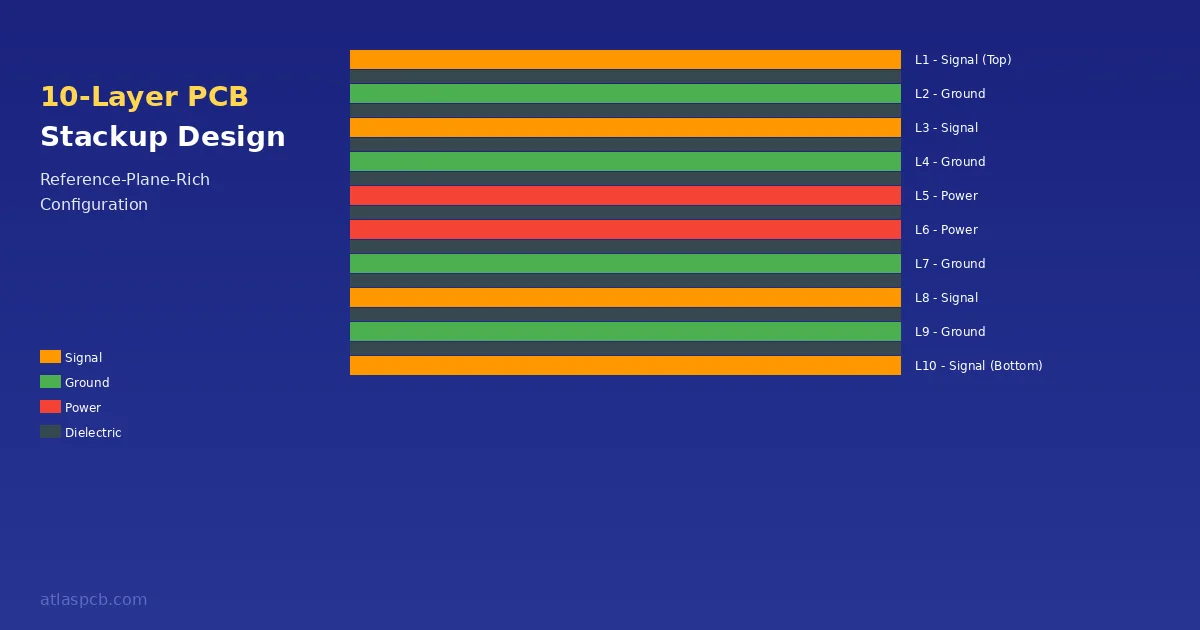
Our 4-layer PCB stackup design guide covers the most common multilayer configuration for designs with moderate routing density and single high-speed interface requirements. If your current 8-layer design seems over-engineered, that guide provides the analysis framework for determining whether 4 layers suffice.
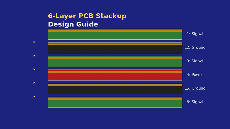
The 6-layer PCB stackup design guide addresses the intermediate complexity level that handles most mixed-signal designs with two or three high-speed interfaces. Many designs that initially appear to need 8 layers can be successfully implemented on 6 layers with careful routing optimization.
For designs requiring even greater complexity — such as high-pin-count FPGA systems, multi-processor server boards, or advanced networking equipment — our 16-layer PCB stackup design guide covers the considerations for moving beyond 8 layers, including sequential lamination planning and advanced HDI via structures.
Engineers working with controlled impedance specifications may also benefit from our impedance-controlled PCB stackup guide which provides detailed calculation methods applicable to any layer count.
Reviewed by AtlasPCB Engineering Team
This article reflects manufacturing practices and specifications current as of August 2026. Stackup configurations, material specifications, and cost estimates are based on our production capabilities and standard material inventory. Specific projects may require customized solutions — contact our engineering team for design-specific recommendations.
About AtlasPCB — We specialize in complex PCB manufacturing for HDI, RF, and high-reliability applications. Explore our impedance-controlled PCB manufacturing, free engineering DFM review, or get an full PCB manufacturing capabilities . Every order includes free engineering review. Get your quote.
Reviewed by AtlasPCB Engineering Team — IPC-certified manufacturing specialists with 15+ years of production experience in HDI, RF, and high-reliability PCB fabrication. Content based on factory floor data and real customer design reviews.
Frequently Asked Questions
What is the best 8-layer PCB stackup configuration?
How much does an 8-layer PCB cost compared to 6-layer?
When should I choose 8 layers instead of 6 layers?
What materials are used in a standard 8-layer PCB stackup?
- 8-layer PCB
- PCB stackup
- stackup design
- impedance control
- multilayer PCB
- PCB manufacturing
- DFM
- signal integrity