· AtlasPCB Engineering · Engineering · 9 min read
5G Antenna PCB Fabrication: Material Requirements and Manufacturing Challenges for mmWave Designs
Detailed engineering guide to 5G mmWave antenna PCB manufacturing covering material selection (Rogers RO3003, RO4350B), Dk tolerance requirements, copper roughness specifications, and registration accuracy for phased array alignment. Covers 24-39 GHz FR2 band applications.
Quick Answer
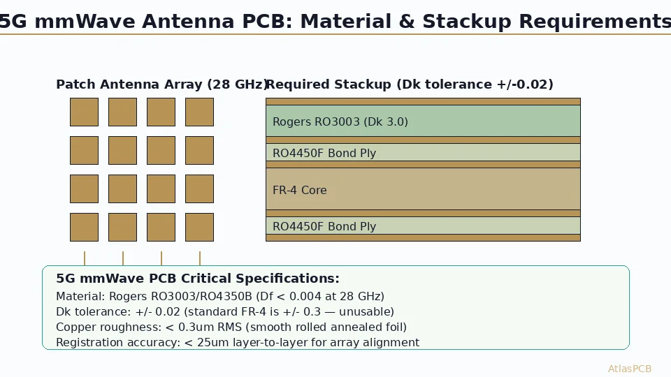
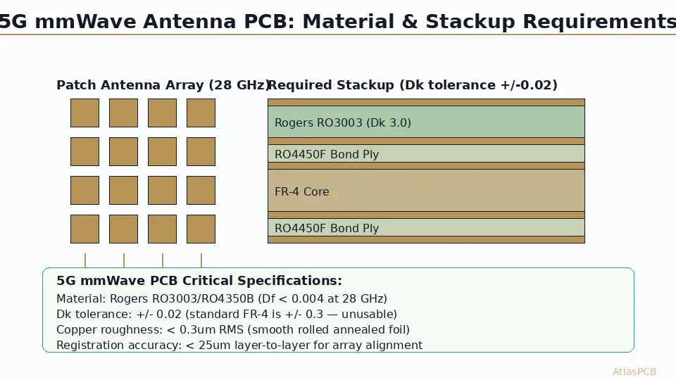
5G mmWave antenna PCBs (24-39 GHz) require Rogers or PTFE-based materials with Df below 0.004 and Dk tolerance of +/-0.02 (versus +/-0.3 on standard FR-4). Critical manufacturing parameters include: copper surface roughness below 0.3um RMS (smooth rolled annealed foil), layer-to-layer registration accuracy below 25um for antenna element alignment, and consistent dielectric thickness control to +/-0.5mil for impedance matching in feed networks. Standard FR-4 is completely unusable at mmWave frequencies due to both excessive loss and Dk instability.
Quick Reference: 5G mmWave PCB Requirements vs Standard PCB
| Parameter | Standard Digital PCB | 5G mmWave Antenna PCB | Why It Matters |
|---|---|---|---|
| Material Dk tolerance | +/-0.3 | +/-0.02 | Phase coherence across array |
| Loss tangent (Df) | 0.020 | < 0.004 | Antenna efficiency |
| Copper roughness | 1.5-2.0um Rz | < 0.5um Rz | Conductor loss at mmWave |
| Layer registration | +/-75um | < 25um | Element position accuracy |
| Dielectric thickness | +/-10% | +/-2% | Impedance in feed network |
| Surface finish | Any | Immersion silver or ENIG | Consistent RF impedance |
If your 5G antenna design requires any frequency above 24 GHz, standard PCB fabrication parameters will not produce a functional board. This is specialist manufacturing requiring RF-specific process controls.
Material Selection for mmWave Frequencies
The material choice for a 5G mmWave antenna PCB is not a preference — it’s a physics constraint. At 28 GHz, electromagnetic waves interact with the PCB dielectric roughly 28 billion times per second, and any material imperfection (glass weave periodicity, resin void, filler particle distribution) creates measurable effects on propagation. This is fundamentally different from digital PCB design, where the dielectric is essentially a structural spacer between copper layers.
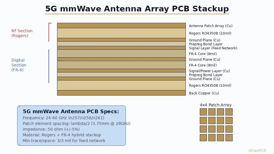
The dominant material system for 5G mmWave antennas in production today is Rogers RO3003 for the antenna/radiating layer and Rogers RO4350B for lower-frequency feed distribution layers. The RO3003’s ceramic-filled PTFE construction delivers Dk of 3.00 with variation of only +/-0.04 across temperature (-40 to +150C) and lot-to-lot — crucial for maintaining consistent antenna element impedance across manufacturing runs and environmental conditions.
In our facility, we maintain incoming material inspection records for every Rogers lot, verifying that Dk measured at 10 GHz falls within the material specification. We’ve seen occasional lots where Dk drifts 0.03-0.05 units from the nominal — still within Rogers’ spec, but enough to shift antenna resonant frequency by 200-400 MHz at 28 GHz. For customers running production volumes, we segregate lots and characterize each batch before committing to their antenna panel builds.
The cost of RO3003 is approximately 5-8x standard FR-4 per square meter of laminate. However, for a typical 5G small cell antenna module (50x50mm, 6-layer hybrid), the material cost differential adds $15-25 per board — a trivial fraction of the system value given that the antenna determines the entire radio’s performance.
CHINA RF PCB MANUFACTURER
Rogers Material In Stock for 5G Antenna Builds
RO3003, RO4350B, and RO4450F in standard thicknesses ready for your mmWave antenna prototype. Hybrid Rogers/FR-4 stackups are our specialty.
View RF Capabilities ›
Copper Roughness: The Hidden Performance Killer
At mmWave frequencies, the skin depth in copper drops below 0.5um — meaning RF current flows within the first half-micron of the conductor surface. Any surface roughness on the same scale as the skin depth directly increases conductor loss through increased effective path length. This phenomenon, negligible at 1 GHz, becomes the dominant loss mechanism at 28+ GHz.
Standard electrodeposited (ED) copper foil has surface roughness (Rz) of 1.5-3.0um on the bonding side — roughened intentionally to improve adhesion to the laminate. At 28 GHz, this roughness increases conductor loss by 30-50% compared to a theoretically smooth conductor. For antenna PCBs where every 0.5 dB of loss directly reduces radiated power (and thus cell coverage), this is unacceptable.
The solution is low-profile or very-low-profile copper foil: reverse-treated (RTF) or hyper-VLP copper with Rz below 0.5um on the signal-carrying side. Rogers’ own LoPro foil and Circuit Foil’s TF foil achieve Rz of 0.3-0.5um while maintaining adequate peel strength (4+ lb/in) through specialized bonding treatments. In our production, we specify VLP copper for all mmWave layers and verify roughness through cross-section measurement on process validation panels.
The trade-off is adhesion. Smoother copper bonds less strongly to the substrate, increasing the risk of pad lifting during assembly rework or thermal cycling. For production 5G antenna modules that will never be reworked (soldered once in automated assembly), this trade-off is acceptable. For prototype boards that may undergo multiple component-level rework cycles, we recommend RTF foil as a middle ground — rougher than VLP but much smoother than standard ED.
Registration Accuracy for Phased Array Alignment
A 5G mmWave phased array antenna works by precisely controlling the phase of each radiating element to electronically steer the beam. Element position errors translate directly to phase errors, which degrade beam pattern — increasing sidelobes, reducing gain, and potentially creating blind spots in the coverage pattern.
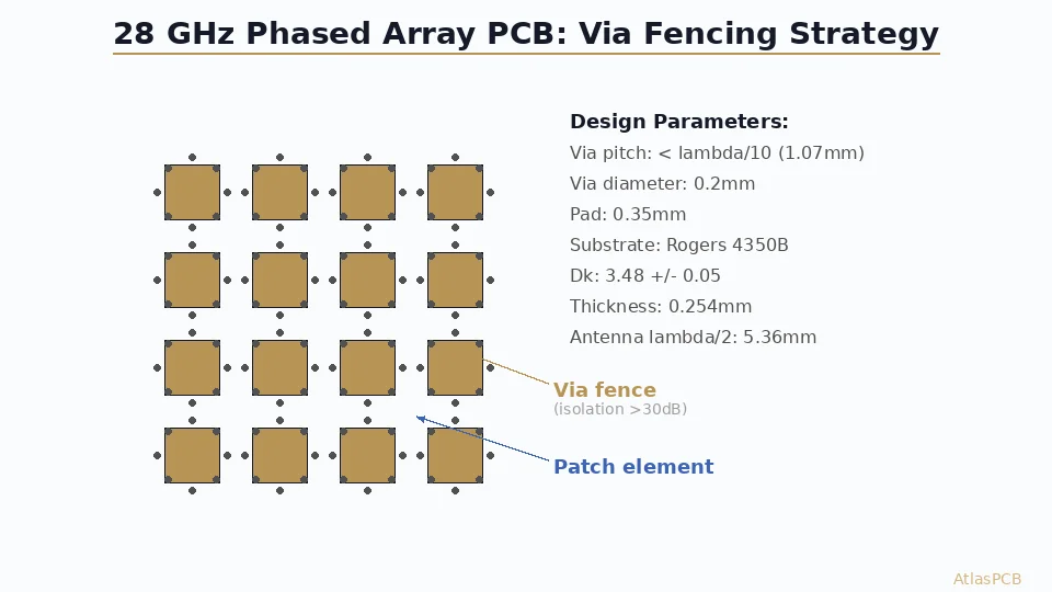
For a 28 GHz 4x4 patch array with half-wavelength spacing (5.36mm between elements), position error of just 0.25mm creates a 16-degree phase error at the outermost elements — enough to raise first sidelobes by 3-4 dB and reduce main beam gain by 0.5-1 dB. Our production specification for 5G antenna panels requires layer-to-layer registration of 25um or better, verified by automated optical inspection (AOI) against the reference Gerber.
Achieving sub-25um registration requires several process controls that standard PCB fabrication does not typically employ: optical alignment marks on every layer (not just outer layers), LDI (laser direct imaging) exposure for both copper and solder mask patterning (eliminating film stretch/shrink errors), and controlled-atmosphere lamination that minimizes panel movement during cure. We also maintain tighter panel size tolerances for Rogers materials, because their lower CTE means less dimensional compensation is needed — but also less margin for error if compensation factors are incorrect.
For 39 GHz and above (where element spacing drops to 3.85mm), even 25um registration may be marginal. At these frequencies, some manufacturers move to sequential lamination approaches where the antenna layer is patterned last (after all inner layers are registered), minimizing the cumulative registration error stack.
PRECISION MANUFACTURING
Sub-25um Registration for Antenna Arrays
LDI patterning, optical registration, and controlled lamination processes deliver the positional accuracy 5G phased arrays demand.
Discuss Your Antenna Design ›Manufacturing Process Differences for mmWave PCBs
Beyond material and registration, several process steps differ fundamentally for mmWave antenna PCBs compared to standard boards:
Drilling: Rogers materials drill differently from FR-4. The ceramic filler is highly abrasive — drill bit life is 30-50% shorter than on FR-4. We use diamond-coated or specially treated carbide bits for Rogers, running at lower spindle speeds (60-80% of FR-4 parameters) to prevent delamination of the ceramic-polymer matrix at the hole wall. Via plating adhesion on Rogers also requires modified desmear chemistry — standard permanganate processes don’t etch the hydrocarbon resin effectively.
Etching: Achieving tight trace width control (+/-0.5mil) on antenna elements requires fine-tuning etch chemistry and using differential etching techniques. The antenna patch dimensions directly set resonant frequency — a patch that should be 3.45mm wide at 28 GHz shifts by 300 MHz if etching removes an additional 0.02mm per side. Our process uses image-etch-measure-compensate cycles with SPC tracking to maintain antenna element dimensional accuracy.
Surface finish: For mmWave boards, the surface finish on RF traces affects impedance and loss. HASL (hot air solder leveling) is unsuitable — the uneven tin surface creates impedance discontinuities. ENIG provides flat, consistent impedance but adds 0.3-0.5um of nickel that slightly increases loss at mmWave. Immersion silver gives the lowest loss (no magnetic material in the RF path) but has limited shelf life. We recommend immersion silver for boards going directly to assembly, and ENIG for boards requiring extended storage.
RF PCB DESIGN AND MANUFACTURING
End-to-End 5G Antenna PCB Capability
From material selection consultation through fabrication, test, and panel-level RF verification. We build mmWave antenna PCBs for production — not just prototypes.
Get Recommendation ›Application Landscape: Where 5G mmWave Antenna PCBs Ship
The primary applications driving demand for mmWave antenna PCB fabrication in 2026 are:
5G small cells (28/39 GHz n257/n260): Outdoor urban densification nodes requiring 64-element or 128-element phased arrays. Board sizes typically 100x100mm to 200x200mm, 6-10 layer hybrid Rogers/FR-4 stackups, production volumes of 10,000-100,000 units per year per operator deployment phase.
Fixed wireless access (FWA) customer premises equipment: Indoor/outdoor units for home broadband replacement, requiring compact 16-64 element arrays with integrated beamforming ICs. These boards demand excellent thermal management (copper coin inserts or thick copper planes for PA heat spreading) alongside RF performance.
Automotive V2X radar integration (60/77 GHz): While technically above our primary 5G focus, the fabrication techniques overlap substantially. Automotive radar PCBs at 77 GHz use similar Rogers/PTFE materials with even tighter tolerance requirements, and the volume projections (millions per year for Level 3+ autonomous vehicles) are driving significant investment in mmWave PCB manufacturing capacity globally.
In our production mix, 5G antenna-related orders have grown 60% year-over-year since 2024, now representing 15% of our total RF PCB revenue. The complexity is high but the value per board makes it economically attractive — and the technical barrier to entry prevents commodity competition from threatening margins.
ATLASPCB
Building a 5G mmWave Antenna? Let's Talk Fabrication.
Upload your antenna design files for detailed material recommendation and quote. Our RF process engineers have built antenna PCBs for 5G infrastructure OEMs across 24-39 GHz bands.
Get Instant Quote ›
Reviewed by AtlasPCB Engineering Team — 15+ years in advanced PCB fabrication for RF, HDI, and rigid-flex applications.
Related Reading:
About AtlasPCB — We specialize in complex PCB manufacturing for HDI, RF, and high-reliability applications. Explore our RF and high-frequency PCB services, Rogers RO4350B PCB manufacturing, or get an full PCB manufacturing capabilities . Every order includes free engineering review. Get your quote.
Reviewed by AtlasPCB Engineering Team — IPC-certified manufacturing specialists with 15+ years of production experience in HDI, RF, and high-reliability PCB fabrication. Content based on factory floor data and real customer design reviews.
Frequently Asked Questions
Why can't FR-4 be used for 5G mmWave antennas?
What materials are used for 5G mmWave antenna PCBs?
How tight does registration need to be for phased array PCBs?
Can hybrid Rogers/FR-4 stackups be used for 5G antenna boards?
- 5G PCB
- mmWave antenna
- Rogers PCB
- phased array
- antenna PCB manufacturing
- RF PCB
- 5G antenna fabrication