· AtlasPCB Engineering · Engineering · 10 min read
5G Antenna PCB Fabrication: Via Fencing and Material Strategy for 28 GHz Phased Arrays
Engineering guide to 5G mmWave antenna PCB manufacturing — covering Rogers 4350B substrate selection, via fencing isolation requirements, array element spacing, and fabrication tolerances for 28 GHz phased array designs.
Quick Answer
5G 28 GHz phased array PCBs require Rogers 4350B substrate (Dk=3.48, 10mil thickness for 50-ohm feed), via fencing with pitch below lambda/10 (1.07mm at 28 GHz) using 0.2mm drill vias, and fabrication tolerances of +/-0.5mil on etch to maintain antenna element performance across the array — making these boards among the most demanding RF PCB manufacturing jobs in current production.
Quick Reference: 28 GHz Phased Array PCB Specifications
| Parameter | Requirement | Manufacturing Tolerance |
|---|---|---|
| Substrate | Rogers 4350B, 10 mil (0.254mm) | Dk 3.48 +/-0.05 |
| Patch element | 2.68mm x 2.68mm (half-wave) | Etch accuracy +/-0.5 mil |
| Element spacing | 5.36mm (lambda/2 free space) | Position +/-1 mil |
| Via fence pitch | <1.07mm (lambda/10 in substrate) | Drill position +/-2 mil |
| Via drill | 0.2mm diameter | +/-0.025mm |
| Via pad | 0.35mm diameter | Registration +/-1 mil |
| Feed network impedance | 50 ohm microstrip (12.5 mil wide) | +/-5% impedance |
| Array size | 4x4 to 16x16 elements | Depends on gain requirement |
| Isolation (element-to-element) | >30 dB | Verified with VNA |
The 28 GHz band (26.5-29.5 GHz for 5G NR FR2) presents the tightest fabrication tolerances of any commercial PCB application currently in volume production. A 1 mil error in patch element width shifts resonant frequency by approximately 200 MHz — potentially moving the antenna response outside the target band. This is why 5G antenna PCB fabrication demands specialist manufacturers with RF-specific process controls.
Substrate Selection: Why Rogers 4350B Dominates at 28 GHz
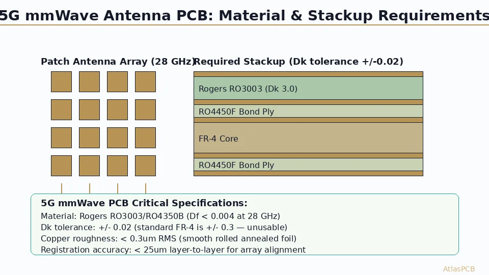
At millimeter-wave frequencies, the dielectric material defines antenna performance more than any other single factor. The substrate’s dielectric constant (Dk) determines element dimensions and feed line geometry. Its loss tangent (Df) determines antenna efficiency and gain. And its Dk uniformity across the panel determines whether all elements in your array resonate at the same frequency — which is the difference between a functional phased array and an expensive paperweight.
Rogers 4350B has become the de facto standard for commercial 28 GHz phased arrays for several engineering reasons that go beyond its datasheet numbers. First, its thermoset hydrocarbon ceramic chemistry provides Dk stability across temperature that PTFE-based alternatives cannot match. The Dk shift from -40C to +85C is less than 1% for 4350B, versus 2-3% for RT5880. For a phased array that must operate in outdoor environments (base stations, CPE units, automotive V2X), this thermal stability prevents beam squinting as temperature changes.
Second, the moisture absorption of 0.06% means Dk remains stable in humid environments. We have tested boards stored at 85C/85% RH for 1000 hours with less than 0.5% Dk drift — within the measurement uncertainty. PTFE materials (like RT5880 at 0.02% moisture absorption) are slightly better, but the difference is academic for properly conformal-coated assemblies.
Third — and this is the manufacturing advantage that most RF engineers underappreciate — Rogers 4350B processes identically to FR-4 on standard equipment. No sodium-naphthenate etch for bonding, no plasma treatment for via preparation, no special drill program beyond feed rate adjustment. This means any manufacturer equipped for Rogers can produce 4350B antenna boards without capital investment in PTFE-specific equipment. The practical benefit: shorter lead times, lower NRE, and more suppliers to choose from.
In our production facility, we process Rogers 4350B daily on the same lines as FR-4 multilayer. The key process adjustments are drill feed rate (30% slower than FR-4 due to ceramic filler abrasiveness), lamination pressure (slightly lower to prevent Rogers compression changing thickness), and etch chemistry (standard cupric chloride works perfectly, but etch factor is slightly different requiring empirical calibration per thickness).
5G ANTENNA PCB MANUFACTURING
28 GHz Phased Array PCBs on Rogers 4350B
We process Rogers 4350B daily with +/-0.5 mil etch accuracy and +/-2 mil via registration. From 4x4 evaluation boards to 16x16 production arrays.
Quote Antenna PCB ›
Via Fencing: The Manufacturing Challenge Nobody Talks About
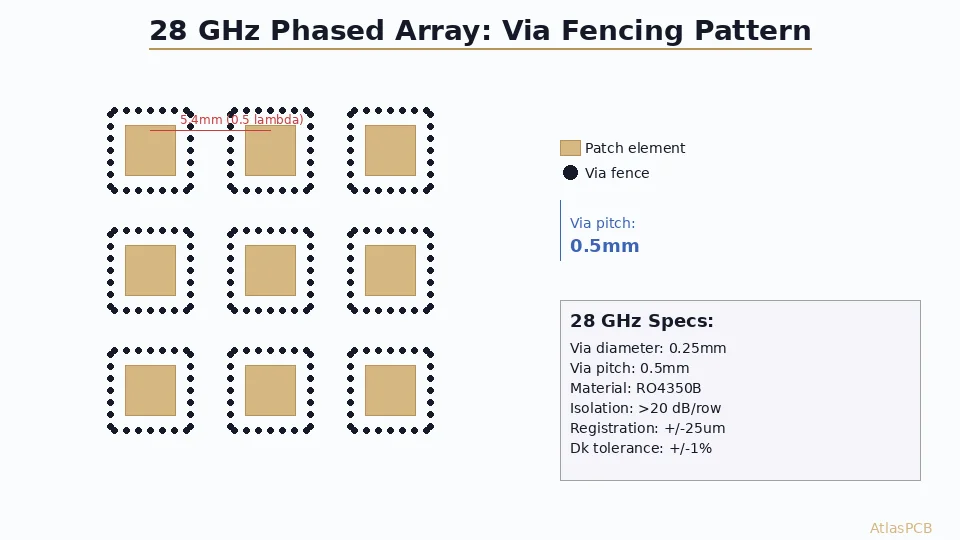
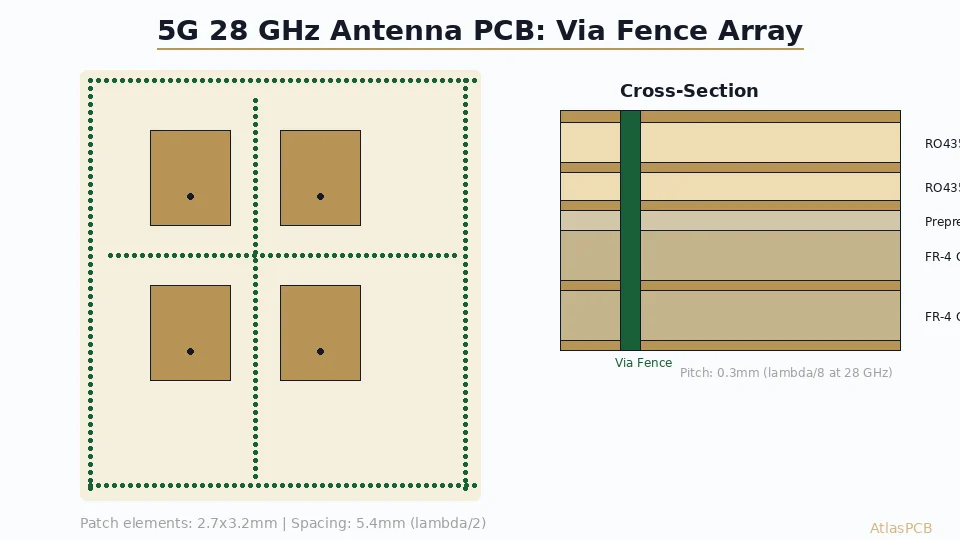
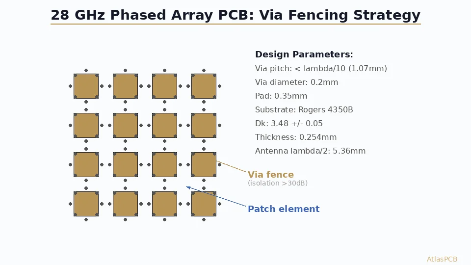
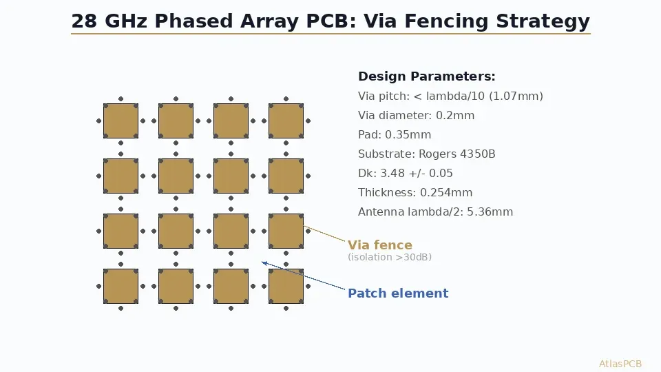
Via fencing in phased array PCBs serves a dual purpose: electrical isolation between elements (suppressing surface wave coupling) and mechanical function as part of a substrate-integrated waveguide (SIW) structure. The physics requirement is straightforward — via pitch must be less than lambda/10 in the substrate medium to prevent electromagnetic leakage between fenced regions.
At 28 GHz in Rogers 4350B (Dk=3.48), the guided wavelength is approximately 5.74mm, making the maximum via pitch 0.574mm. Practical designs use 0.5-0.8mm pitch as a compromise between isolation performance and drill density. A 4x4 array with via fencing around each element requires approximately 400-600 vias just for isolation — on top of the feed network vias, ground stitching, and connector transition vias. A 16x16 array can require 5000+ vias on a board smaller than a credit card.
The manufacturing challenge is positional accuracy of these vias relative to the antenna elements. A via fence that is shifted 1-2 mils relative to the patch element creates asymmetric coupling that degrades the antenna’s co-pol/cross-pol isolation and can introduce unexpected beam tilt. Our CNC drill machines hold +/-2 mil positional accuracy, which is adequate for most 28 GHz designs, but the most demanding military-grade arrays specify +/-1 mil — requiring our newest laser-positioned mechanical drill platforms.
Drill aspect ratio is another constraint. At 0.2mm drill diameter through a 0.254mm Rogers 4350B substrate, the aspect ratio is only 1.27:1 — trivial from a drilling standpoint. But when the antenna PCB is part of a multilayer hybrid stack (Rogers on top for antenna, FR-4 below for beamformer), the total board thickness may reach 1.5-2.0mm, giving aspect ratios of 7.5-10:1 for the fencing vias. This pushes against the limits of standard mechanical drilling for 0.2mm holes and may require laser-assisted pilot holes or alternative via formation techniques.
Feed Network Design and Impedance Control
The corporate feed network that distributes RF power to each antenna element is arguably more demanding to fabricate than the antenna elements themselves. A 4x4 array requires a 1:16 power divider network with precisely controlled impedance at every junction. At 28 GHz, a quarter-wave transformer section is only 1.43mm long in Rogers 4350B — meaning the feed network occupies very little board area but demands extreme dimensional accuracy.
For 50-ohm microstrip on 10 mil Rogers 4350B with 1 oz copper (35um after plating): the trace width is 12.5 mil (0.318mm). A quarter-wave transformer to match 50 ohms to 100 ohms (for a Wilkinson divider T-junction) requires a 70.7-ohm section at 8.5 mil width. The difference between these two impedance values is only 4 mil of trace width — well within manufacturing capability, but demanding consistent etch factor across the entire feed network.
In our process, we achieve this through Laser Direct Imaging (LDI) rather than phototool-based exposure. LDI eliminates the dimensional instability of film phototools (which can stretch 1-2 mil across a panel due to humidity and temperature) and provides consistent 0.5 mil registration to the drill pattern. For 28 GHz antenna boards specifically, we recommend (and usually require) LDI imaging to achieve the feed network accuracy that phased array performance demands.
The transition from microstrip feed network to the antenna patch itself requires attention to parasitic inductance at the feed point. Inset-fed patches (where the microstrip feeds into a slot cut into the patch edge) provide impedance matching without quarter-wave transformers but require very precise slot dimensions — typically 0.3-0.8mm deep by 0.15-0.25mm wide. These features are at the edge of standard etch resolution and may require selective high-resolution imaging on the feed region.
CHINA RF PCB MANUFACTURER
LDI Imaging for mmWave Accuracy
Laser Direct Imaging with +/-0.5 mil registration. Essential for 28 GHz feed networks where 1 mil of trace width variance changes impedance by 3-4 ohms.
RF Manufacturing ›Testing and Verification: Proving Array Performance
Fabrication of the antenna PCB is only half the challenge. Verifying that all elements resonate correctly and the feed network distributes power uniformly requires RF measurement capabilities that most PCB manufacturers do not offer. Here is what a proper antenna PCB verification flow looks like:
In-process verification (done during fabrication):
- Cross-section microscopy of via fence geometry (3 coupons per panel)
- Impedance testing of feed network traces (TDR, all controlled impedance traces)
- Etch dimension measurement on patch elements (+/-0.5 mil pass/fail)
- Copper thickness uniformity across array area (+/-10% thickness variation)
Post-fabrication RF verification (done on finished boards):
- Return loss (S11) measurement at array input port: must show resonance at 28 GHz +/-200 MHz
- Element-to-element coupling (S21 between ports on multi-port arrays): must be below -25 dB
- Near-field scan (if customer provides test fixture): validates element excitation uniformity
We offer in-process verification as standard on all antenna PCB orders and can coordinate with the customer’s RF test lab for post-fabrication characterization. For volume production, we establish process qualification based on the first article — once fabrication parameters are locked (etch time, drill feed, lamination cycle), subsequent panels receive coupon-based verification plus statistical process control on critical dimensions.
RF PCB TESTING
In-Process RF Verification Included
TDR impedance testing, cross-section analysis, and dimensional measurement on every antenna PCB production lot. RF characterization data provided with shipment.
Test Capabilities ›DFM Checklist for 5G Antenna PCB Designers
Before submitting your 28 GHz antenna design to any manufacturer, verify these critical parameters:
Material specification: Specify Rogers 4350B by name (not “equivalent” — equivalents have different Dk values). Include required thickness (6.6 or 10 mil), copper type (ED standard or RA rolled for lowest roughness), and copper weight (typically 0.5 oz for minimum surface roughness at mmWave).
Via fence completeness: Ensure every element has complete via fencing around its ground plane boundary. Gaps in via fencing — even 2-3 missing vias — create leakage paths that degrade isolation by 10-15 dB. Our DFM review checks for fence continuity as a standard step.
Ground plane integrity: The ground reference plane (L2 in a typical antenna stackup) must be solid copper with no routing, splits, or clearance holes under the antenna array area. Any ground plane discontinuity directly impacts antenna impedance and radiation pattern.
Edge clearance: Maintain minimum 3x substrate thickness clearance from any antenna element to the board edge. At 10 mil substrate, that means 0.75mm minimum (we recommend 2mm for robust performance). Board edge reflections can create unwanted sidelobes in the array pattern.
Connector transition: The SMA/SMPM/U.FL connector footprint should include a grounded coplanar waveguide (GCPW) transition section at least 2mm long between the connector and the microstrip feed network. This transition structure must be part of your design file — we fabricate exactly what you submit.
ATLASPCB
Building 5G Antenna Hardware?
From evaluation arrays to production phased array antennas. Rogers 4350B in stock, LDI imaging standard, TDR verification on every board.
Start 5G Antenna Project ›
Reviewed by AtlasPCB Engineering Team — 15+ years in advanced PCB fabrication for RF, HDI, and rigid-flex applications.
Related Reading:
About AtlasPCB — We specialize in complex PCB manufacturing for HDI, RF, and high-reliability applications. Explore our RF and high-frequency PCB services, or get an Rogers RO4350B PCB manufacturing . Every order includes free engineering review. Get your quote.
Reviewed by AtlasPCB Engineering Team — IPC-certified manufacturing specialists with 15+ years of production experience in HDI, RF, and high-reliability PCB fabrication. Content based on factory floor data and real customer design reviews.
Frequently Asked Questions
What PCB material is best for 28 GHz phased array antennas?
Why is via fencing necessary in 5G antenna PCBs?
What via pitch is required for 28 GHz isolation?
Can standard PCB manufacturers fabricate 28 GHz antenna boards?
- 5g-pcb
- antenna-pcb
- rf-manufacturing
- phased-array