· AtlasPCB Engineering · News · 7 min read
TSMC CoWoS and InFO Driving PCB-Substrate Convergence: What PCB Manufacturers Need to Know
TSMC's advanced packaging technologies are blurring the boundary between IC substrates and PCBs. As L/S requirements approach 5/5 μm, PCB manufacturers must adapt or risk obsolescence.
The Line Between IC Substrate and PCB Is Disappearing
For decades, the printed circuit board industry and the IC substrate industry operated in distinct technological lanes. PCBs handled board-level interconnection with feature sizes measured in mils, while IC substrates managed the fine-pitch world between the silicon die and the package. That separation is rapidly dissolving.
TSMC’s advanced packaging platforms — particularly Chip-on-Wafer-on-Substrate (CoWoS) and Integrated Fan-Out (InFO) — are driving a convergence that is redefining what “substrate” and “PCB” mean. As these technologies proliferate beyond their initial AI accelerator niche into networking, HPC, automotive, and consumer applications, the implications for traditional PCB manufacturers are profound.
Understanding the Packaging Landscape
To appreciate the convergence, it helps to understand what TSMC’s key packaging technologies actually do:
CoWoS (Chip-on-Wafer-on-Substrate). CoWoS uses a silicon or organic interposer to connect multiple chiplets (such as GPU dies and HBM memory stacks) in a 2.5D configuration. The interposer provides ultra-fine-pitch redistribution layers (RDL) with line/space as tight as 0.4/0.4 μm, enabling the thousands of interconnections required between chiplets.
The CoWoS assembly sits on a large organic substrate — and this is where the convergence begins. The organic substrate beneath a CoWoS package must support:
- BGA ball pitches of 0.65–1.0 mm
- Line/space of 8/8 μm to 5/5 μm in advanced variants
- 10–16 redistribution layers
- Panel sizes approaching 70 mm × 70 mm for large packages like NVIDIA’s B200 and AMD’s MI350
InFO (Integrated Fan-Out). InFO eliminates the need for a separate interposer by embedding the die directly in a fan-out package with RDL built up around it. InFO-based packages achieve smaller form factors and better electrical performance for mobile and automotive applications.
CoWoS-L (Local Silicon Interconnect). TSMC’s latest variant uses smaller local silicon interconnect (LSI) bridges instead of a full silicon interposer, reducing cost while maintaining fine-pitch die-to-die connectivity. CoWoS-L further increases the demand on the underlying organic substrate, as more of the routing complexity shifts from the interposer to the substrate layers.
Where PCB and Substrate Converge
The convergence manifests in several dimensions:
Feature Size Overlap
Traditional PCBs operate with minimum line/space of 75/75 μm (3/3 mil) in standard production, with [HDI PCB capabilities]/blog/hdi-pcb-design-guide/) pushing to 50/50 μm (2/2 mil) or occasionally 40/40 μm. IC substrates, meanwhile, have operated at 10/10 μm to 5/5 μm.
The gap is narrowing from both sides. Advanced PCB processes like mSAP (modified Semi-Additive Process) now achieve 25/25 μm in production. Meanwhile, the organic substrates used beneath CoWoS packages are pushing from 10/10 μm toward 8/8 μm and 5/5 μm — feature sizes that increasingly require semiconductor-like lithographic processes.
This creates a continuum rather than a clear dividing line:
| Technology Level | L/S (μm) | Traditional Domain |
|---|---|---|
| Standard PCB | 75–100 | PCB |
| HDI PCB | 40–75 | PCB |
| Advanced HDI (mSAP) | 20–40 | PCB/Substrate overlap |
| IC Substrate | 8–15 | Substrate |
| Advanced Substrate | 5–8 | Substrate |
| Silicon RDL | 0.4–2 | Semiconductor |
Material Convergence
The materials used in advanced substrates and high-performance PCBs are increasingly similar. Both use:
- Low-Dk, low-Df dielectric build-up films (ABF — Ajinomoto Build-up Film being the dominant substrate material)
- Electroless copper seed layers with electrolytic copper plating
- Laser-drilled microvias with via-in-pad architectures
- Similar solder mask and surface finish technologies
The primary difference is that substrate manufacturing uses ABF film in a sequential build-up process optimized for <15 μm features, while PCB manufacturing uses prepreg and laminate systems optimized for larger features. But as PCB manufacturers adopt ABF-compatible processes and substrate makers scale to larger panel formats, the process technology overlap increases.
Equipment and Process Convergence
The manufacturing equipment required for advanced substrates and cutting-edge PCBs is converging:
- Laser direct imaging (LDI) systems capable of 5 μm resolution are used in both domains
- Sputtering for copper seed layers, once exclusive to substrate manufacturing, is being adopted by advanced PCB shops
- Semi-additive processing (SAP/mSAP) for fine-line patterning is used across both industries
- Plasma desmear and advanced via cleaning share common equipment platforms
What This Means for PCB Manufacturers
The convergence creates both threats and opportunities for traditional PCB manufacturers:
The Threat: Margin Compression in the Middle
PCB manufacturers that focus on standard-complexity boards face growing competition from both directions. Substrate manufacturers are scaling to larger panel formats and could theoretically produce high-end PCBs more efficiently. Meanwhile, low-cost Asian PCB manufacturers are moving up the technology curve, compressing margins for mid-tier fabricators.
The Opportunity: Advanced Packaging Support
The explosive growth in CoWoS and InFO packaging creates demand for ecosystem components that PCB manufacturers are well-positioned to supply:
Test boards and interposer test substrates. Every CoWoS package requires test infrastructure — probe cards, burn-in boards, and test sockets — that use advanced PCB technology with [controlled impedance]/blog/controlled-impedance-pcb/) and high layer counts.
Package-level redistribution. As CoWoS-L shifts routing from silicon interposers to organic substrates, PCB manufacturers with mSAP capability can address the growing substrate demand.
System-level PCBs for advanced packages. The motherboards and system boards that host CoWoS-packaged devices must themselves meet stringent requirements for power delivery, [signal integrity]/blog/signal-integrity-pcb-design-guide/), and thermal management. NVIDIA’s GB200 NVL72 server tray, for example, uses a PCB with 20+ layers, ultra-low-loss materials, and back-drilled vias — pushing the capabilities of even advanced PCB fabricators.
Heterogeneous integration boards. Emerging architectures that combine multiple packages on a single board — sometimes called “board-level fan-out” — require PCB manufacturers who understand both board-level and substrate-level design rules.
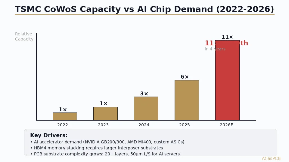
TSMC’s Packaging Roadmap and Industry Impact
TSMC’s packaging revenue has grown at over 30% annually since 2023, driven primarily by AI accelerator demand from NVIDIA, AMD, and Broadcom. The company’s 2026 roadmap includes:
- CoWoS-S Gen 5: Supporting reticle sizes up to 3.3× (approximately 100mm × 75mm), enabling larger multi-chiplet configurations
- CoWoS-L Gen 2: Improved LSI bridge technology with higher interconnect density
- InFO-3D: Stacked die configurations for mobile and automotive applications
- SoIC (System on Integrated Chips): True 3D chip stacking with through-silicon vias (TSVs)
Each generation places increasing demands on the organic substrate beneath the package. Industry analysts at Yole Intelligence estimate that the advanced packaging substrate market will reach $18 billion by 2028, growing at 22% CAGR.
Investment Requirements
For PCB manufacturers seeking to participate in the substrate convergence, the investment threshold is substantial:
- mSAP line: $30–50 million for a production-capable modified semi-additive processing line
- Sputtering equipment: $5–10 million per sputtering system for seed layer deposition
- Advanced LDI: $2–5 million per high-resolution laser direct imaging system
- Clean room upgrades: Class 1000 or better clean room environments, versus Class 10,000 typical for advanced PCB production
- Metrology: Advanced optical and X-ray inspection systems capable of resolving <10 μm features
Several major PCB manufacturers have already made these investments. Unimicron, AT&S, Ibiden, and Shinko Electric are positioning themselves as dual-capability manufacturers serving both PCB and substrate markets.
The Role of Materials Innovation
[Material selection]/blog/pcb-material-selection-guide/) is becoming a critical differentiator in the convergence space. Key material trends include:
- ABF film alternatives: Several companies are developing lower-cost alternatives to Ajinomoto’s dominant ABF build-up film, potentially democratizing access to fine-line substrate manufacturing
- Glass core substrates: Glass offers superior dimensional stability, lower warpage, and higher wiring density compared to organic cores, making it attractive for large CoWoS substrates
- Low-CTE dielectrics: Matching the coefficient of thermal expansion (CTE) between the silicon die and the substrate is critical for reliability, driving demand for new dielectric formulations
Outlook for the Industry
The PCB-substrate convergence is not a future possibility — it is happening now. TSMC’s advanced packaging volumes are growing rapidly, and every package shipped requires substrate and PCB support infrastructure. For the traditional PCB industry, the message is clear: the manufacturers that invest in finer-feature capabilities, cleaner processes, and substrate-compatible technologies will capture growing markets. Those that don’t will find their addressable market shrinking as packaging technology continues to advance.
The convergence also creates opportunities for new business models, including PCB manufacturers offering substrate co-design services, fab-lite approaches where PCB companies handle substrate prototyping while specialized foundries handle volume production, and regional supply chain strategies that pair [PCB manufacturing]/blog/pcb-manufacturing-process-15-steps/) with substrate capabilities.
Atlas PCB is investing in advanced manufacturing capabilities to support the evolving demands of high-performance packaging and system integration applications.
Atlas PCB provides advanced PCB manufacturing with HDI, controlled impedance, and high-layer-count capabilities for next-generation packaging applications. Request a quote for your next project.
About AtlasPCB — We specialize in complex PCB manufacturing for HDI, RF, and high-reliability applications. Explore our full PCB manufacturing capabilities, or get an instant online quote . Every order includes free engineering review. Get your quote.
Reviewed by AtlasPCB Engineering Team — IPC-certified manufacturing specialists with 15+ years of production experience in HDI, RF, and high-reliability PCB fabrication. Content based on factory floor data and real customer design reviews.
- news
- advanced-packaging
- tsmc
- cowos
- substrate