· AtlasPCB Engineering · News · 4 min read
Advanced Packaging Revolution: How Chiplets and 2.5D Integration Are Reshaping PCB Substrates
The shift to chiplet-based architectures and 2.5D/3D packaging is creating new demands for PCB substrates, blurring the boundary between traditional PCBs and semiconductor packaging with implications for materials, design rules, and manufacturing processes.
The semiconductor industry’s accelerating adoption of chiplet-based architectures is sending ripple effects through the entire electronics supply chain—and PCB substrate manufacturers are at the epicenter of this transformation.
The Chiplet Paradigm Shift
The monolithic die approach that dominated semiconductor design for decades is giving way to disaggregated chiplet architectures. Instead of fabricating a single large die, companies are designing smaller functional blocks (chiplets) that are interconnected through advanced packaging technologies.
Major implementations in 2026 include:
- AMD Zen 6 processors: Multiple compute chiplets connected via silicon interposer
- Intel Arrow Lake and successors: Tile-based architecture with Foveros 3D stacking
- NVIDIA Blackwell: Multi-die GPU package with HBM integration
- Apple M5 series: Chiplet design with UltraFusion interconnect
- Qualcomm Snapdragon X Elite successors: Heterogeneous chiplet integration
Impact on PCB Substrates
Chiplet packages create new requirements for the PCB substrates they mount to:
Finer Escape Routing
Chiplet packages typically have higher ball density than monolithic packages because the package needs to route signals between chiplets AND between the package and the PCB. Ball pitches of 0.4mm and below are becoming standard, requiring HDI substrates with microvia-based escape routing.
For designers working with these packages, our [HDI stackup design guide]/blog/hdi-pcb-stackup-design-advanced/) covers the escape routing considerations in detail.
Thermal Management Challenges
Chiplet packages can exceed 500W TDP, concentrated in a relatively small area. The PCB substrate must participate in thermal management:
- Thermal via arrays under the package with 0.3mm vias on 1.0mm pitch
- Internal copper planes dedicated to heat spreading
- Low-CTE materials to manage thermal-mechanical stress at the package-to-board interface
- Warpage control — the board must remain flat enough for reliable BGA soldering
Signal Integrity at the Package-Board Interface
UCIe (Universal Chiplet Interconnect Express), the emerging standard for chiplet-to-chiplet communication, operates at extremely high data rates. While UCIe signals stay within the package, the associated I/O signals (PCIe Gen 6, CXL 3.0, DDR5/6) that reach the PCB substrate are equally demanding.
The PCB substrate must provide:
- Controlled differential impedance (85–100Ω ±7%) on fine-pitch escape routes
- Via stub elimination through back-drilling or blind via construction
- Low-loss dielectric materials (Df <0.005 at 10 GHz)
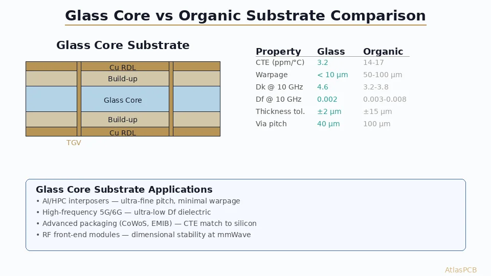
The Interposer-to-PCB Transition
2.5D packaging uses silicon or organic interposers between the chiplets and the PCB. The organic interposer—essentially an ultra-fine-line substrate—is manufactured using processes closer to semiconductor packaging than traditional PCB fabrication:
- Line/space: 2/2µm to 10/10µm (vs. 50/50µm for advanced PCB)
- Via diameter: 20–50µm (vs. 75–150µm for PCB microvias)
- Layer count: 4–8 redistribution layers
However, this interposer must still connect to a conventional PCB through a BGA interface, and the PCB must route all signals to memory, power regulators, and other board-level components.
The Emerging “Bridge” Substrate
A new category of substrate is emerging between traditional PCBs and IC substrates:
| Attribute | Traditional PCB | Bridge Substrate | IC Substrate |
|---|---|---|---|
| Line/space | ≥50/50µm | 15–50µm | 2–15µm |
| Via diameter | ≥75µm | 30–75µm | 10–30µm |
| Layer count | 4–68 | 8–20 | 4–12 RDL |
| Process | Subtractive | SAP/mSAP | SAP |
| Dk requirement | Standard-low | Low-very low | Very low-ultra low |
| Panel size | 18”×24” | 12”×18” | 6”×8” (strip) |
PCB manufacturers capable of mSAP (modified Semi-Additive Process) and fine-line imaging are positioning themselves to serve this emerging market segment.
Industry Investment
The global investment in advanced packaging substrate capacity reflects the urgency of this trend:
- Japan: Ibiden, Shinko investing $2B+ in high-density substrate capacity
- Taiwan: Unimicron, AT&S Taiwan expanding mSAP-capable lines
- South Korea: Samsung Electro-Mechanics, LG Innotek scaling substrate production
- China: Domestic manufacturers accelerating capability development for chiplet substrates
What This Means for PCB Designers
- Stackup complexity increases: The PCB connected to a chiplet package may need more routing layers for escape routing, even if the overall system is not more complex
- Material specifications tighten: Low-loss, dimensionally stable materials become mandatory for boards hosting chiplet packages
- DFM engagement must be earlier: The tight tolerances required for chiplet-compatible substrates demand close collaboration between IC package designers, PCB designers, and substrate fabricators from the initial architecture phase
- Hybrid manufacturing: Some boards may require both traditional PCB areas and mSAP fine-line areas, creating manufacturing challenges
At Atlas PCB, we are investing in fine-line imaging and mSAP processing capabilities to support the advanced packaging transition. For current projects requiring fine-pitch BGA escape routing and low-loss materials, request a quote to discuss your substrate requirements.
The chiplet revolution is not just a semiconductor story—it’s fundamentally reshaping what we expect from PCB substrates, and the PCB industry is evolving rapidly to meet these new demands.
About AtlasPCB — We specialize in complex PCB manufacturing for HDI, RF, and high-reliability applications. Explore our full PCB manufacturing capabilities, or get an instant online quote . Every order includes free engineering review. Get your quote.
Reviewed by AtlasPCB Engineering Team — IPC-certified manufacturing specialists with 15+ years of production experience in HDI, RF, and high-reliability PCB fabrication. Content based on factory floor data and real customer design reviews.
- news
- advanced packaging
- chiplet
- 2.5D
- substrate
- interposer