· News · 3 min read
Advanced Packaging Drives PCB Substrate Convergence — Chiplet Era Demands New Interconnect Approaches
As chiplet architectures and advanced packaging reshape semiconductor design, the boundary between IC substrate and PCB is blurring. Here's what it means for PCB engineers and manufacturers.
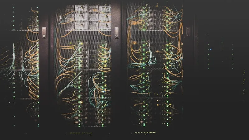
The semiconductor industry’s shift toward chiplet-based architectures is fundamentally changing what’s expected of the printed circuit board sitting underneath. As interposers, bridge dies, and fan-out packaging push interconnect density to levels previously reserved for silicon, PCB manufacturers are being asked to deliver capabilities that blur the line between traditional circuit board and IC substrate.
The Convergence Trend
Historically, the electronics stack had clear boundaries:
- Die level: nm-scale features, silicon substrate
- Package substrate: µm-scale features, organic/ceramic substrate
- PCB: tens-of-µm features, FR-4 or specialty laminate
In 2026, these boundaries are compressing. TSMC’s CoWoS (Chip-on-Wafer-on-Substrate) and Intel’s EMIB (Embedded Multi-die Interconnect Bridge) demand organic substrates with 2-5 µm line/space — capabilities that were IC substrate territory just five years ago.
The PCB, in turn, must now interface with these advanced packages at pad pitches of 0.4-0.5 mm (vs. traditional 1.0-1.27 mm for older BGA packages), requiring [HDI manufacturing]/blog/hdi-pcb-stackup-design-advanced-en/) with [microvia technology]/blog/pcb-laser-drilling-microvia-technology-en/) that approaches substrate-level precision.
What’s Driving This?
AI Accelerator Demand
Every major AI training GPU (NVIDIA H200/B200, AMD MI400, Google TPUv6) uses multi-chiplet designs connected through advanced packaging. The host PCB must:
- Support 4000-6000+ pin BGA sockets
- Deliver power at 500-1000A per package
- Maintain signal integrity at 112 Gbps PAM4 per lane
- Manage 500-1000W of thermal dissipation
High-Performance Computing
Datacenter CPUs have moved to chiplet architectures (AMD EPYC Genoa/Turin, Intel Granite Rapids). The supporting PCBs require:
- 20+ layer constructions with [controlled impedance]/blog/pcb-impedance-matching-differential-pairs-en/)
- Ultra-low-loss materials (Df <0.003 at 28+ GHz)
- Embedded capacitance and [power integrity]/blog/pcb-power-integrity-decoupling-en/) structures
- Back-drilling for stub elimination in high-speed channels
Automotive ADAS
Advanced driver assistance systems package multiple sensor-processing chiplets together, requiring automotive-qualified PCBs with HDI capabilities and [reliability standards]/blog/ipc-standards-pcb-classes-en/) (IPC-6012 DA).
PCB Manufacturing Implications
Trace/Space Requirements Tightening
The escape routing challenge from 0.4mm-pitch advanced packages requires:
- 50 µm (2 mil) trace/space minimum for inner layers
- Microvia drill diameters of 75-100 µm
- Registration accuracy of ±12.5 µm or better
These are at the edge of what conventional PCB processes can achieve. Manufacturers investing in mSAP (modified Semi-Additive Process) can achieve 25-30 µm trace/space — bridging into substrate territory.
Material Requirements
Advanced package PCBs demand:
- Low-CTE cores (matched to package CTE to reduce warpage)
- [Low-Dk/Df laminates]/blog/pcb-high-speed-material-dk-df-comparison-en/) for signal integrity
- Ultra-flat copper foils (RTF or VLP profiles) for fine-line imaging
- Controlled resin content for consistent dielectric thickness
Quality and Reliability
The value of components on these boards ($5,000-50,000+ per package) makes board defects catastrophically expensive. Manufacturing requires:
- 100% [electrical testing]/blog/pcb-electrical-testing-flying-probe-vs-fixture-en/) at tighter continuity thresholds
- Automated optical inspection with AI-enhanced defect classification
- Microsection process monitoring with statistical process control
- Full lot traceability from raw material to finished board
The Industry Response
PCB Manufacturers Upgrading
Major PCB fabricators in Asia (Unimicron, Zhen Ding, AT&S) are investing billions in capacity that bridges traditional PCB and IC substrate manufacturing:
- mSAP lines for 25-50 µm features
- ABF (Ajinomoto Build-up Film) processing
- Panel-level substrate manufacturing
- Cleaner room environments (Class 100-1000 vs. traditional Class 10,000)
New Supply Chain Dynamics
The convergence is reshaping the competitive landscape:
- Traditional substrate makers (Ibiden, Shinko) expanding downward into advanced PCB
- Traditional PCB makers expanding upward into substrate-like capabilities
- New entrants specializing in the “middle ground” (advanced HDI + substrate-like precision)
What PCB Engineers Should Do Now
- Expect tighter specifications: Package suppliers will increasingly specify PCB requirements that push capability boundaries
- Invest in HDI expertise: [Via-in-pad]/blog/pcb-via-in-pad-plated-over-design-en/), stacked microvias, and mSAP processes are becoming table stakes
- Plan for longer lead times: Advanced capability PCBs require specialized manufacturers with limited capacity
- Engage fab early: DFM review at schematic/placement stage, not after routing, to ensure manufacturability
AtlasPCB’s Position
We’re investing in advanced HDI capabilities to support the chiplet transition, including 3-level stacked microvias, 50µm trace/space capability, and hybrid material processing. For designs requiring advanced package support, reach out for a capability assessment — our engineering team can evaluate your specific requirements and recommend an optimal fabrication approach.
About AtlasPCB — We specialize in complex PCB manufacturing for HDI, RF, and high-reliability applications. Explore our full PCB manufacturing capabilities, or get an instant online quote . Every order includes free engineering review. Get your quote.
Reviewed by AtlasPCB Engineering Team — IPC-certified manufacturing specialists with 15+ years of production experience in HDI, RF, and high-reliability PCB fabrication. Content based on factory floor data and real customer design reviews.
- industry news
- advanced packaging
- chiplets
- IC substrate
- PCB substrate convergence
- interposer