· AtlasPCB Engineering · News · 6 min read
Glass Core Substrates: Next-Generation PCB Technology Poised to Transform AI Chip Packaging
Major semiconductor companies are advancing glass core substrate technology for next-generation AI chip packaging, promising superior signal integrity and higher interconnect density. Here's what this shift means for the broader PCB manufacturing ecosystem.
Glass Core Substrates: Next-Generation PCB Technology Poised to Transform AI Chip Packaging
A quiet revolution is underway in the world of advanced electronics packaging, and it starts with a material most people associate with windows, not semiconductors: glass.
Multiple major semiconductor manufacturers have announced significant progress on glass core substrate technology in the first quarter of 2026, positioning it as the critical enabler for next-generation AI accelerators and high-performance computing chips. The technology promises to overcome fundamental limitations of current organic substrates — and its ripple effects will be felt throughout the PCB manufacturing supply chain.
Why Glass, Why Now?
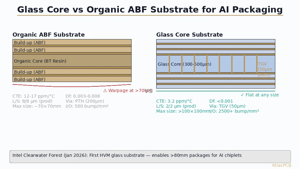
The AI hardware boom has pushed chip packaging to its limits. Current-generation AI accelerators — the massive processors powering large language models and data center inference — use organic ABF (Ajinomoto Build-up Film) substrates as the interposer layer between the silicon die and the main printed circuit board.
These organic substrates have served the industry well, but they’re hitting physical walls:
Dimensional instability: Organic substrates have a coefficient of thermal expansion (CTE) of 12–17 ppm/°C, significantly higher than silicon’s 2.6 ppm/°C. This mismatch causes warpage during thermal cycling, limiting the density of solder bumps connecting the die to the substrate. As AI chips grow larger — some now exceeding 800mm² — the warpage problem becomes acute.
Interconnect pitch limitations: Current organic substrates reliably support bump pitches down to approximately 130–150μm. Next-generation AI chips require pitches below 100μm to accommodate the massive I/O counts needed for chiplet-to-chiplet communication.
Signal integrity at high frequencies: As data rates between chips and memory climb past 50 Gbps per lane, the dielectric loss of organic materials (typically Df of 0.003–0.008) becomes a meaningful performance limiter.
Glass addresses all three challenges simultaneously.
The Properties That Make Glass Compelling
Glass core substrates offer a compelling set of physical and electrical properties:
- CTE of ~3.2 ppm/°C — closely matched to silicon, dramatically reducing warpage and enabling ultra-fine pitch interconnects
- Dielectric loss (Df) below 0.001 at frequencies relevant to next-gen packaging, enabling cleaner high-speed signal transmission
- Surface flatness within ±1μm — far superior to organic substrates, allowing advanced lithographic patterning of redistribution layers
- Through-glass vias (TGVs) with pitches as fine as 50μm, compared to 200μm+ for typical through-mold vias in organic substrates
- Excellent mechanical rigidity — glass panels resist handling-induced deformation during manufacturing
The net effect: glass cores can support 2–3x the interconnect density of current organic substrates while delivering superior electrical performance.
Industry Progress in 2026
Several major players have made notable announcements:
Intel presented detailed process flow data at a packaging conference in March 2026, demonstrating glass core substrates with functional 76μm-pitch copper pillar interconnects. The company described glass as “the inevitable next step” for its advanced packaging roadmap beyond 2027.
Samsung’s packaging division has been developing glass core technology in parallel, with published results showing successful integration of high-bandwidth memory (HBM) stacks on glass interposers. The company targets limited production qualification by Q4 2026.
Major substrate manufacturers in Japan and Taiwan have invested in glass panel processing lines, adapting semiconductor lithography equipment for the unique requirements of glass substrate fabrication — including laser drilling for TGVs and specialized metallization processes for copper adhesion to glass surfaces.
What This Means for Traditional PCB Manufacturing
While glass core substrates operate at the package level — between the chip and the PCB — their adoption creates significant downstream effects for [PCB material selection]/blog/pcb-material-selection-guide/) and design:
1. Tighter PCB-side requirements
As package substrates achieve finer interconnect pitches, the PCBs they mount to must keep pace. Expect increasing demand for [HDI PCB technology]/blog/hdi-pcb-technology/) with microvia pitches below 200μm, pad-on-via designs, and tighter impedance tolerance (±5% rather than ±10%) on signal layers interfacing with glass-substrate packages.
2. New thermal management demands
Glass has lower thermal conductivity than organic substrates (~1 W/mK vs. ~0.3 W/mK for typical organics — better, but still modest). PCB designers will need to incorporate more aggressive thermal via arrays and copper coin solutions in the regions directly beneath glass-substrate packages.
3. Material compatibility considerations
The CTE mismatch between glass substrates (3.2 ppm/°C) and standard FR-4 PCBs (14–17 ppm/°C) is significant. For high-reliability applications, this may drive adoption of low-CTE PCB materials or specialized interposer layers at the PCB-package interface.

Challenges Remaining
Glass substrate technology is not without hurdles:
- Cost: Glass core substrates are currently estimated at 3–5x the cost of equivalent organic substrates. Volume production and process maturation will be needed to close this gap.
- Fragility: Despite its rigidity, glass is brittle. Handling and processing glass panels through existing manufacturing infrastructure requires significant equipment modification and new process controls.
- Supply chain immaturity: The glass substrate supply chain is nascent. Specialized glass compositions, TGV drilling equipment, and metallization chemistries are produced by a limited number of suppliers, creating potential bottleneck risks.
- Standards: Industry standards for glass substrate specifications, reliability testing, and quality classification are still under development within IPC and JEDEC working groups.
The Timeline and PCB Industry Implications
Based on current industry roadmaps:
- Late 2026–Early 2027: First limited-volume glass core substrates in premium AI accelerator packages
- 2028–2029: Broader adoption in high-performance computing, with organic substrates remaining dominant for consumer and automotive electronics
- 2030+: Potential cost parity enabling wider deployment; mainstream PCB manufacturers may begin offering glass-compatible HDI capabilities as a standard service
For PCB engineers and designers, the key takeaway is not that glass will replace your boards — it won’t. But glass core substrates will raise the bar for PCB quality and precision at the package interface, making [advanced HDI capabilities]/blog/hdi-pcb-technology/) increasingly essential for cutting-edge electronic system designs.
The glass core substrate revolution is coming. The PCB manufacturers who prepare now — investing in finer-pitch capabilities, tighter process control, and advanced material expertise — will be the ones best positioned to serve the AI hardware market of 2028 and beyond.
AtlasPCB Engineering tracks emerging packaging technologies and their implications for PCB manufacturing. Visit atlaspcb.com for technical resources and manufacturing capabilities.
About AtlasPCB — We specialize in complex PCB manufacturing for HDI, RF, and high-reliability applications. Explore our full PCB manufacturing capabilities, or get an instant online quote . Every order includes free engineering review. Get your quote.
Reviewed by AtlasPCB Engineering Team — IPC-certified manufacturing specialists with 15+ years of production experience in HDI, RF, and high-reliability PCB fabrication. Content based on factory floor data and real customer design reviews.
- industry-news
- advanced-packaging
- glass-substrate
- ai-chips
- pcb-technology