· AtlasPCB Engineering · News · 4 min read
Samsung Expands ABF Substrate for AI Chips
Samsung Electro-Mechanics invests $1.2B in ABF substrate capacity to meet surging AI chip packaging demand from NVIDIA and AMD.
Samsung Electro-Mechanics Bets Big on ABF Substrates
Samsung Electro-Mechanics (SEMCO) has announced a $1.2 billion investment to expand its ABF (Ajinomoto Build-up Film) substrate production capacity, targeting the surging demand for advanced chip packaging driven by AI accelerator processors. The investment will fund new production lines at SEMCO’s existing facilities in Sejong, South Korea, and Thái Nguyên, Vietnam, with volume production expected by Q3 2027.
The expansion represents SEMCO’s largest single capital expenditure in its substrate division’s history and signals the company’s strategic pivot toward AI-driven semiconductor packaging — a market segment experiencing unprecedented growth.
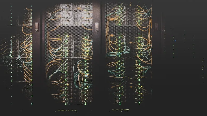
The ABF Substrate Bottleneck
ABF substrates are the unsung heroes of modern computing. Every high-performance processor — from NVIDIA’s Blackwell GPUs to AMD’s EPYC server CPUs to custom AI accelerators from Google, Amazon, and Microsoft — relies on ABF substrates to bridge the gap between nanometer-scale silicon and millimeter-scale PCB features.
The fundamental challenge: AI chips are getting larger (some exceeding 800 mm²), with more I/O connections (over 10,000 bumps), requiring higher signal speeds (up to 112 Gbps per lane). Each of these trends demands more sophisticated ABF substrates with:
- Finer line/space geometries (down to 15/15 µm for next-gen designs)
- More layers (12–20 layers for high-end AI packages)
- Larger substrate sizes (up to 80 × 80 mm for large-die packages)
- Tighter registration accuracy (±8 µm or better)
The result is a persistent supply-demand imbalance. Industry analysts at TechInsights estimate that global ABF substrate demand will grow 25% annually through 2028, while capacity additions — despite billions in investment — will grow only 18–20% annually.
Investment Details
SEMCO’s $1.2 billion investment breaks down as follows:
Sejong, South Korea ($700 million): Expansion of the existing Sejong campus with a new cleanroom facility dedicated to next-generation ABF substrates with sub-20 µm features. This facility will use mSAP (modified semi-additive process) technology for the finest layers, combined with conventional SAP for build-up layers. Target: 15,000 substrate panels per month.
Thái Nguyên, Vietnam ($500 million): New production lines at SEMCO’s Vietnamese campus, focusing on mid-range ABF substrates for networking, automotive, and consumer AI applications. This facility will handle 20/20 µm and above features. Target: 25,000 substrate panels per month.
Combined, the new capacity will increase SEMCO’s total ABF substrate output by approximately 35%.
Competitive Landscape
SEMCO is not alone in the ABF substrate investment race. The major competitors are all expanding aggressively:
| Company | Investment | Location | Timeline | Target Capability |
|---|---|---|---|---|
| Ibiden | $1.3B | Ogaki/Aono, Japan | Q4 2026 | 12/12 µm L/S |
| Unimicron | $2.5B | Taoyuan, Taiwan | H1 2027 | 15/15 µm L/S |
| AT&S | €1.7B | Leoben/Kulim | Q2 2027 | 15/15 µm L/S |
| SEMCO | $1.2B | Sejong/Vietnam | Q3 2027 | 15/15 µm L/S |
| Shinko | $800M | Nagano, Japan | Q1 2027 | 18/18 µm L/S |
The total industry investment in ABF substrate capacity exceeds $7 billion for 2025–2028 alone — a remarkable figure for what was, until recently, a niche segment of the electronics manufacturing industry.
Technology Transition: mSAP Goes Mainstream
A key technology shift driving these investments is the transition from subtractive etching to modified semi-additive process (mSAP) for the finest substrate layers. In conventional subtractive processing, trace widths below 25 µm become unreliable due to etch factor limitations. mSAP — which involves depositing a thin copper seed layer, patterning with photoresist, electroplating traces, and flash-etching the seed — enables reliable features below 15 µm.
This same mSAP technology is cascading into [substrate-like PCB (SLP) fabrication]/news/news-sam-substrate-like-pcb-technology-2026/), blurring the traditional boundary between IC substrates and high-end PCBs. Engineers working on designs that push conventional [HDI PCB limits]/blog/hdi-pcb-technology/) should be aware that SLP capabilities are becoming more widely available.
Supply Chain Implications
For PCB engineers and procurement teams, the ABF substrate expansion has several implications:
Lead times remain extended: Despite capacity additions, ABF substrate lead times are expected to remain at 16–24 weeks through 2027. Plan accordingly.
Cost pressures continue: High-end ABF substrates for AI packages cost $50–200+ per unit, and prices are not expected to decline significantly until 2028 when multiple new facilities reach full utilization.
Design-for-supply matters: Engineers should consider ABF substrate availability when selecting package types. Using established feature sizes (20/20 µm and above) rather than bleeding-edge geometries can significantly improve availability and cost.
PCB-substrate co-design is essential: The performance of the ABF substrate and the system PCB are tightly coupled, particularly for power delivery and high-speed signal integrity. [High-speed PCB design]/blog/high-speed-pcb-design/) practices must account for substrate parasitics.
Broader Industry Impact
The ABF substrate boom is pulling investment and talent into the broader PCB ecosystem. Materials suppliers (ABF film from Ajinomoto, ultra-thin copper foil from Mitsui), equipment manufacturers (LDI systems, laser drills, plating lines), and specialty chemical companies are all expanding to support the substrate industry’s growth.
For PCB engineers working on systems that interface with advanced IC packages, understanding the capabilities and limitations of the substrate layer is increasingly important. The substrate is no longer “someone else’s problem” — it directly impacts your PCB design constraints.
To discuss advanced interconnect requirements for your design, upload your Gerbers for a free engineering review or contact Atlas PCB’s engineering team.
Related: [Advanced Packaging Chiplet PCB Substrate]/news/news-advanced-packaging-chiplet-pcb-substrate/) | [Glass Core Substrate PCB AI Chips 2026]/news/news-glass-core-substrate-pcb-ai-chips-2026/) | [PCB Materials Guide]/blog/pcb-materials-guide/)
About AtlasPCB — We specialize in complex PCB manufacturing for HDI, RF, and high-reliability applications. Explore our full PCB manufacturing capabilities, or get an instant online quote . Every order includes free engineering review. Get your quote.
Reviewed by AtlasPCB Engineering Team — IPC-certified manufacturing specialists with 15+ years of production experience in HDI, RF, and high-reliability PCB fabrication. Content based on factory floor data and real customer design reviews.
- industry-news
- abf-substrate
- samsung
- ai-chips
- packaging
- supply-chain