· AtlasPCB Engineering · News · 8 min read
Keysight Advances PCB Signal Integrity Testing with AI-Powered Compliance Suite
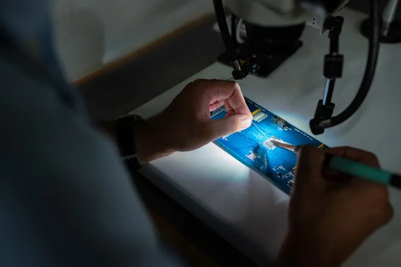
Keysight Technologies unveils an AI-driven signal integrity testing platform that automates high-speed PCB validation, reducing compliance testing time by up to 60%.
A New Era in High-Speed PCB Validation
Keysight Technologies has announced the launch of its PathWave Signal Integrity AI Suite, a comprehensive platform that brings artificial intelligence to the forefront of high-speed PCB compliance testing. Unveiled at DesignCon 2026 in Santa Clara, the suite represents one of the most significant advances in PCB validation tooling in recent years, addressing the growing complexity challenges that engineers face as data rates continue to climb.
The announcement comes at a critical inflection point for the electronics industry. With [PCIe Gen 6]/news/news-pcie-gen6-pcb-design-challenges-2026/) pushing signaling rates to 64 GT/s, DDR5 memory interfaces exceeding 8,800 MT/s, and 800G Ethernet deployments accelerating across data centers, the margin for error in PCB design has shrunk to near zero. Traditional testing approaches — manual setup, sequential compliance checks, and reactive troubleshooting — are struggling to keep pace.
The Challenge of Modern High-Speed Validation
Today’s high-speed digital interfaces operate at frequencies where every aspect of PCB design becomes critical. Trace geometry, via transitions, [stackup configuration]/blog/multilayer-pcb-stackup-design-guide/), material properties, and even the placement of decoupling capacitors can make the difference between a design that passes compliance and one that fails spectacularly.
The testing burden has grown exponentially. A typical PCIe Gen 6 compliance validation can require hundreds of individual measurements across multiple channels, with each measurement demanding precise probe placement, correct termination, and careful de-embedding. For a complex server motherboard with multiple high-speed interfaces, full compliance testing can consume weeks of engineering time.
“We’ve reached a point where the complexity of compliance testing has become a bottleneck in product development,” said Dr. Joachim Peerlings, Vice President of Keysight’s Electronic Industrial Solutions Group, during the DesignCon keynote. “AI is the only practical path to maintaining design velocity.”
Inside the PathWave SI AI Suite
Predictive Failure Analysis
The cornerstone of the new suite is its predictive failure analysis engine. Using machine learning models trained on millions of historical [signal integrity]/blog/signal-integrity-pcb-design-guide/) measurements, the system can analyze a PCB design and predict likely compliance failures before a single physical prototype is built.
The AI engine ingests design data — including Gerber files, stackup definitions, [material parameters]/blog/pcb-high-speed-material-dk-df-comparison/), and net topology — and runs thousands of virtual what-if scenarios in minutes. It then produces a prioritized risk assessment that identifies:
- Impedance discontinuities at via transitions, connector interfaces, and layer changes
- Crosstalk hotspots where aggressive routing density threatens adjacent signal pairs
- Return loss violations caused by impedance mismatches in [controlled impedance]/blog/pcb-impedance-control/) traces
- Insertion loss budgets that may exceed specification limits given the selected [PCB materials]/blog/pcb-material-selection-guide/)
- Power integrity risks from inadequate decoupling or plane resonances
In benchmark testing conducted with three major server OEMs, the predictive engine correctly identified 94% of compliance failures found during subsequent physical testing, with a false positive rate below 8%.
Automated Compliance Testing
For physical validation, the suite introduces fully automated compliance test sequences for major high-speed standards. Engineers connect the device under test, select the target specifications, and the system handles the rest — configuring instruments, positioning measurements, applying de-embedding, and generating compliance reports.
Supported standards at launch include:
- PCIe Gen 5 and Gen 6 (transmitter and receiver compliance)
- DDR5 and LPDDR5X (including write leveling and read training analysis)
- USB4 (all tunnel types and speed modes)
- 800G Ethernet (IEEE 802.3df)
- CXL 3.0 (link layer and transaction layer compliance)
The automation extends beyond simple test execution. The AI system continuously monitors measurement quality during testing, flagging potential issues such as probe contact degradation, environmental interference, or fixture artifacts that could compromise results. When anomalies are detected, the system either automatically compensates or pauses testing and alerts the engineer.
Integration with EDA Workflows
Recognizing that [signal integrity validation]/blog/high-speed-pcb-design/) should begin long before physical prototyping, Keysight has built deep integration with leading EDA platforms. The PathWave SI AI Suite can import designs directly from Cadence Allegro, Altium Designer, and Siemens Xpedition, maintaining full fidelity of stackup definitions, material assignments, and design constraints.
This integration enables a continuous validation loop where engineers can:
- Run predictive analysis during schematic and layout design
- Generate targeted [DFM recommendations]/blog/pcb-dfm-checklist/) based on signal integrity risk assessment
- Create virtual compliance previews before committing to fabrication
- Correlate physical test results back to design models for iterative improvement
Impact on PCB Design and Manufacturing
Shifting Left in the Design Cycle
The introduction of AI-powered predictive testing represents a fundamental shift in the PCB development workflow. Traditionally, signal integrity problems were discovered late in the design cycle — often during physical compliance testing — leading to costly board respins and schedule delays. Each respin of a complex multilayer PCB can cost tens of thousands of dollars and add weeks to the development timeline.
By moving compliance prediction earlier in the design process, the PathWave SI AI Suite enables what Keysight calls “shift-left validation.” Design teams can identify and resolve signal integrity issues during layout, when changes are relatively inexpensive, rather than discovering them during physical testing when options are limited.
Early adopters report significant reductions in design iterations. One hyperscale data center operator involved in the beta program noted a 40% reduction in board respins for their 800G switch designs, attributing the improvement directly to the predictive analysis capabilities.
Implications for PCB Fabrication
The tool’s impact extends beyond design into manufacturing. The predictive engine’s analysis of [impedance sensitivity]/blog/pcb-impedance-control/) and material parameter impact provides fabricators with actionable intelligence about which manufacturing parameters are most critical for a given design.
For example, the system might identify that a particular design is highly sensitive to dielectric thickness variations in layers 3 and 4 but relatively tolerant of trace width variations. This information allows fabricators to focus their process controls where they matter most, improving first-pass yield without imposing unnecessarily tight tolerances across the entire board.
This capability is particularly valuable for HDI PCB manufacturing, where the interaction between microvia structures, thin dielectric layers, and high-frequency signals creates complex impedance control challenges. The AI engine can model these interactions and provide specific fabrication guidance that traditional impedance calculators cannot.
The Role of Material Data
One of the suite’s most innovative features is its material intelligence database, which maintains calibrated high-frequency characterization data for over 500 [PCB laminates and prepregs]/blog/pcb-material-selection-guide/). Rather than relying on datasheet values — which are often measured at a single frequency and may not reflect actual performance at multi-gigahertz operating frequencies — the system uses measured Dk and Df data across the full frequency range of interest.
This material intelligence is critical for accurate [signal integrity prediction]/blog/pcb-high-speed-material-dk-df-comparison/). At PCIe Gen 6 frequencies, the difference between using generic datasheet values and frequency-dependent measured data can mean the difference between a passing and failing insertion loss budget. The database is continuously updated through Keysight’s partnerships with major laminate manufacturers.
Industry Context and Competitive Landscape
The Broader AI-in-EDA Trend
Keysight’s announcement fits within a broader industry trend of applying [AI to PCB design and validation]/news/news-ai-pcb-design-tools-cadence-altium-ml-2026/). Major EDA vendors have been integrating machine learning capabilities across their platforms, from AI-assisted routing to automated [EMI compliance prediction]/blog/emc-emi-pcb-design/).
However, Keysight’s approach is distinctive in its focus on the measurement and testing domain rather than the design domain. By combining AI-driven prediction with physical measurement automation, the company is addressing a gap that pure-software EDA tools cannot fill — the correlation between simulated and actual signal integrity performance.
What This Means for Design Engineers
For PCB design engineers, the practical implications are significant. The PathWave SI AI Suite lowers the expertise barrier for high-speed compliance testing, making it accessible to teams that may not have dedicated signal integrity specialists. At the same time, for experienced SI engineers, the AI capabilities free them from routine testing tasks to focus on more challenging design problems.
The suite also has implications for [PCB testing methodologies]/blog/pcb-testing-methods/) more broadly. As AI-powered tools become standard in the validation workflow, the industry may need to revisit how compliance testing is specified and documented. Standards bodies including the PCI-SIG and USB-IF are already engaging with Keysight and other test equipment manufacturers to explore how AI-assisted testing should be treated in formal compliance programs.
Availability and Pricing
The PathWave Signal Integrity AI Suite is available immediately in two configurations: a software-only predictive analysis package for design teams, and a full hardware-plus-software bundle that includes Keysight’s latest UXR-Series oscilloscopes with integrated AI acceleration. Pricing for the software package starts at $45,000 annually, while the full bundle varies based on bandwidth and channel configuration.
Keysight is also offering a free 90-day evaluation license for the predictive analysis module, allowing design teams to assess the tool’s accuracy against their existing designs and test data.
Looking Forward
As high-speed interfaces continue to push data rates higher — with PCIe Gen 7 and DDR6 already on the horizon — the role of AI in PCB validation will only grow. The complexity of these next-generation standards will make manual testing approaches increasingly impractical, and tools like the PathWave SI AI Suite will likely become essential components of the design workflow.
For PCB designers and manufacturers navigating the challenges of [high-speed design]/blog/high-speed-pcb-design/), the message is clear: AI-powered validation is no longer a future concept — it’s a present-day competitive advantage.
Designing high-speed PCBs that demand tight impedance control and advanced signal integrity? Get a quote from Atlas PCB for expert fabrication of complex multilayer boards optimized for signal performance.
About AtlasPCB — We specialize in complex PCB manufacturing for HDI, RF, and high-reliability applications. Explore our impedance-controlled PCB manufacturing . Every order includes free engineering review. Get your quote.
Reviewed by AtlasPCB Engineering Team — IPC-certified manufacturing specialists with 15+ years of production experience in HDI, RF, and high-reliability PCB fabrication. Content based on factory floor data and real customer design reviews.
- news
- pcb-industry
- signal-integrity
- testing
- eda-tools