· AtlasPCB Engineering · News · 7 min read
PCIe Gen 6.0 Finalization Brings New PCB Design Challenges for 64 GT/s Signaling
The PCIe 6.0 specification pushes data rates to 64 GT/s with PAM4 encoding, imposing stringent new requirements on PCB materials, via design, trace geometry, and signal integrity that will reshape server and GPU interconnect board design.
PCIe Gen 6.0 Finalization Brings New PCB Design Challenges for 64 GT/s Signaling
PCI Express 6.0 has moved from specification to silicon. With major controller and retimer chips from Broadcom, Marvell, and Microchip sampling to server OEMs throughout 2026, the industry is confronting a reality that signal integrity engineers have been warning about for two years: the PCB is now the bottleneck.
At 64 GT/s per lane using PAM4 (Pulse Amplitude Modulation, 4 levels) encoding, PCIe 6.0 doubles the bandwidth of Gen 5 while operating at the same 32 GHz Nyquist frequency. But PAM4’s three-level eye opening has inherently 9.5 dB less noise margin than NRZ (Non-Return-to-Zero) encoding. That margin loss must be recovered somewhere — and the PCB channel is where designers have the most work to do.
The Insertion Loss Wall
The fundamental challenge is channel insertion loss. The PCIe 6.0 specification defines a total channel loss budget of approximately 36 dB at 32 GHz for a full-length (12-inch) CEM connector topology. After accounting for connector loss, package escape routing, and silicon TX/RX equalization capability, the PCB trace and via budget is typically constrained to 20–25 dB at 32 GHz.
For context, a standard FR-4 laminate (Df ≈ 0.020 at 10 GHz) introduces roughly 1.0–1.2 dB/inch of insertion loss at 32 GHz for typical 5-mil trace on inner layers. Over a 6-inch trace, that’s 6–7 dB just from dielectric loss — before accounting for copper roughness, via transitions, and connector interfaces. The math simply doesn’t work with commodity materials.
The industry’s response is a wholesale migration to ultra-low-loss and extremely-low-loss laminates for PCIe 6.0 channels:
- Panasonic Megtron 7 (R-5785N): Dk ≈ 3.3, Df ≈ 0.002 at 10 GHz — the current workhorse for 112G SerDes and now the baseline for PCIe 6.0.
- Isola Tachyon 100G: Dk ≈ 3.02, Df ≈ 0.0021 at 10 GHz — positioned as a direct Megtron 7 competitor with slightly lower Dk enabling thinner dielectric builds.
- Rogers RO4835T: Dk ≈ 3.33, Df ≈ 0.0030 at 10 GHz — a thermoset option compatible with standard FR-4 processing, offering a middle ground between cost and performance.
These materials reduce dielectric loss to 0.4–0.6 dB/inch at 32 GHz, roughly halving the loss compared to mid-loss alternatives like Megtron 6 or IS680. For detailed guidance on selecting high-frequency substrates, our [substrate selection guide covering Dk and Df]/blog/high-frequency-pcb-substrate-selection-dk-df/) provides a comprehensive framework.
Copper Roughness: The Hidden Loss Contributor
At 32 GHz, conductor loss from copper roughness becomes a dominant factor. Standard electrodeposited (STD) copper foil has an Rz roughness of 8–10 μm, which at high frequencies effectively increases the electrical path length and adds significant loss through the skin effect.
PCIe 6.0 designs mandate HVLP (Hyper Very Low Profile) or HVLP2 copper, with Rz values below 3 μm and ideally below 2 μm. The Hammerstad-Jensen or Huray roughness models used in channel simulation show that switching from STD to HVLP2 copper saves 0.15–0.25 dB/inch at 32 GHz — a meaningful improvement when the total budget is measured in single digits.
However, HVLP and HVLP2 copper present manufacturing challenges. Lower roughness means reduced mechanical adhesion to the laminate, potentially affecting peel strength during lamination and through thermal cycling. PCB fabricators must carefully balance copper treatment processes — oxide replacement, silane coupling agents — to maintain adhesion without reintroducing roughness.
Via Stubs: Zero Tolerance at 32 GHz
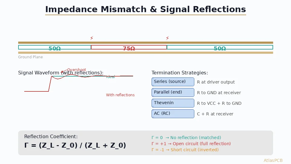
Via stubs — the unused portion of a plated through-hole extending beyond the signal layer — have always been a [signal integrity concern in high-speed design]/blog/signal-integrity-pcb-design-guide/). At PCIe 6.0 frequencies, they become fatal.
A via stub acts as a quarter-wave resonant structure. A 20-mil stub resonates at approximately 19 GHz, placing a deep null directly in the PCIe 6.0 operating band. Even a 10-mil stub creates a resonance at 38 GHz that degrades the channel response within the Nyquist bandwidth.
The specification effectively requires via stubs shorter than 5–8 mils for compliant channels. This is achieved through three methods:
Back-drilling — mechanically removing the stub after plating. Modern CNC back-drill equipment achieves ±3 mil depth accuracy, enabling stub control to within 5 mils of the signal layer. Our [technical guide on PCB back-drilling]/blog/pcb-back-drill/) covers the process in detail.
Blind and buried vias — designing via structures that only span the required layers, eliminating stubs entirely. This adds manufacturing complexity and cost but provides the best electrical performance.
Via-in-pad with back-drill — for BGA escape routing, via-in-pad designs combined with back-drilling offer the most compact high-speed routing solutions.
At Atlas PCB, back-drilling with depth control to ±4 mils is a standard capability across our [high-speed PCB production]/blog/high-speed-pcb-design/), supporting the demanding via stub requirements of 56G and 112G SerDes designs.
Trace Geometry: Tighter Than Ever
PCIe 6.0 tightens impedance tolerance requirements to ±5% for differential pairs (100Ω ±5Ω), compared to the ±10% commonly accepted for Gen 4 and Gen 5. Achieving this requires:
Trace width control within ±0.5 mil (12.5 μm). For a typical 4-mil trace width targeting 100Ω differential impedance, this means the fabricator must hold 3.5 to 4.5 mils consistently across the panel. This pushes against the limits of standard subtractive etch processes and is driving adoption of modified semi-additive (mSAP) or advanced etch compensation techniques for high-speed PCB layers.
Dielectric thickness control within ±0.5 mil. Impedance is highly sensitive to dielectric spacing — a 1-mil change in prepreg thickness can shift impedance by 5–8Ω. PCB fabricators serving the PCIe 6.0 market are investing in laser-based thickness measurement and closed-loop lamination press controls.
Glass weave effect mitigation. Standard E-glass woven fabric creates periodic Dk variations as traces cross over and between glass bundles. At 32 GHz, these variations cause measurable skew and impedance fluctuations. PCIe 6.0 designs commonly specify spread glass (1035, 1067, or 1078 styles), mechanically spread or flat glass, or NE-glass (lower Dk glass formulations) to minimize this effect.
PAM4 and the Manufacturing Quality Imperative
NRZ signaling is relatively forgiving of manufacturing variation — the eye opening is large, and equalization can compensate for moderate channel impairments. PAM4 at 32 GBaud is not.
The three-level PAM4 eye has an opening approximately one-third the size of NRZ at the same baud rate. This means every manufacturing defect — a slight impedance discontinuity from a resin-starved area, a micro-void in a via barrel, a localized Dk variation from uneven glass distribution — has three times the relative impact on signal quality.
This is driving PCB fabricators to implement tighter process controls specifically for PCIe 6.0 boards:
- 100% impedance testing on every coupon, with TDR (Time Domain Reflectometry) validation of actual trace impedance rather than calculated values.
- Cross-section analysis at increased frequency to verify dielectric thickness, copper plating uniformity, and via barrel quality.
- Insertion loss testing using vector network analyzer (VNA) measurements on test coupons matched to production panel builds, verifying that the actual Df and surface roughness meet design assumptions.
The Ecosystem Impact
PCIe 6.0’s PCB requirements are not limited to server motherboards. The specification affects every board in the signal chain:
- GPU and accelerator cards — NVIDIA’s next-generation accelerators and AMD’s Instinct series will use PCIe 6.0 x16 interfaces requiring add-in card PCBs with the same material and via requirements.
- Storage controllers and NVMe backplanes — high-density NVMe storage arrays with PCIe 6.0 x4 lanes per drive require backplane PCBs handling dozens of high-speed channels simultaneously.
- Switch and retimer cards — PCIe switch fabrics from Broadcom and Microchip require mid-board carrier PCBs that maintain channel integrity through multiple connector hops.
- Test and validation equipment — ATE and protocol analyzer PCBs must exceed production board quality to serve as reference channels.
Looking Ahead
PCIe 7.0, already in development at PCI-SIG targeting 128 GT/s, will push these challenges further — likely requiring optical or very short reach (VSR) copper links for anything beyond a few inches. But PCIe 6.0 represents the current frontier where conventional copper PCB technology must perform at its absolute limit.
For design teams and procurement engineers specifying PCIe 6.0 boards in 2026, the message is clear: material selection, via management, and fabricator capability are no longer secondary considerations. They are the primary determinants of whether your channel will close.
Ready to start your project? Upload your Gerbers for a free engineering review, or talk to an engineer about your design requirements.
About AtlasPCB — We specialize in complex PCB manufacturing for HDI, RF, and high-reliability applications. Explore our impedance-controlled PCB manufacturing . Every order includes free engineering review. Get your quote.
Reviewed by AtlasPCB Engineering Team — IPC-certified manufacturing specialists with 15+ years of production experience in HDI, RF, and high-reliability PCB fabrication. Content based on factory floor data and real customer design reviews.
- industry-news
- pcie-gen6
- high-speed
- signal-integrity
- server-pcb