· AtlasPCB Engineering · Engineering · 10 min read
PCB DFM Check: Panel Utilization Optimization — Design Adjustments That Cut Manufacturing Cost 15-25%
Practical guide to optimizing PCB panel utilization during DFM review. Covers board outline adjustments, rail sizing, breakaway tab placement, and array configuration strategies that maximize panel yield and reduce per-unit cost by 15-25% without changing your circuit design.
Quick Answer
PCB panel utilization — the percentage of panel area occupied by usable boards — directly determines your per-unit manufacturing cost. Moving from 65% to 85% utilization by adjusting board dimensions by 1-3mm, optimizing rail width, or rotating board orientation can reduce cost 15-25% without any circuit design change. This is the single highest-impact DFM check that most engineers skip because it requires coordination with your manufacturer's panel size.
Quick Reference: Panel Utilization Impact on Cost
| Utilization | Boards per Panel (example 50x30mm board) | Relative Cost per Board |
|---|---|---|
| 60% | 48 | 1.33x (baseline wasteful) |
| 70% | 56 | 1.14x |
| 80% | 64 | 1.00x (good) |
| 85% | 68 | 0.94x |
| 90% | 72 | 0.89x |
Every 5% increase in panel utilization reduces per-unit cost by approximately 5-6%. Over production volumes of 1,000-10,000 boards, this compounds into thousands of dollars saved.
Why Panel Utilization Is the Most Overlooked DFM Check
Most PCB DFM reviews focus on trace/space violations, annular rings, and solder mask clearances — all important, but these are binary pass/fail checks. Panel utilization, by contrast, is a continuous optimization that directly scales your unit cost, yet most engineers never think about it because their CAD tool does not show the manufacturing panel.
In our facility, we review approximately 400 new part numbers per month. Roughly 30% of incoming designs have panel utilization below 70% — meaning more than 30% of every manufacturing panel becomes scrap. When we flag these to customers and suggest board outline adjustments, about half can accommodate changes that improve utilization by 10-20%. On a 5,000-piece order at $8/board, a 20% utilization improvement saves $1,600 in material costs alone — often more than the NRE tooling fee.
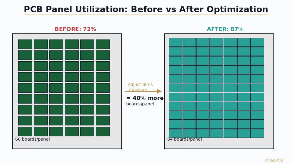
The fundamental equation is simple: your unit cost is (panel processing cost) / (boards per panel). Every factory operation — imaging, etching, plating, drilling, testing — is performed per panel regardless of how many boards fit on it. Fitting 72 boards instead of 60 on the same panel reduces your per-unit share of every processing step by 20%.
FREE DFM OPTIMIZATION
We Optimize Your Panel Layout Before Quoting
Upload your Gerber files and our CAM team will show you the panel layout with utilization percentage — and suggest dimension adjustments if applicable.
Upload Gerbers ›
The Five Optimization Levers for Panel Utilization
1. Board Outline Dimension Adjustment (Impact: 5-20%)
This is the highest-impact change and the one most engineers resist because it feels like “changing the design.” In reality, most PCB outlines have 2-5mm of dimensional margin that exists because someone drew a round number in the mechanical CAD without checking panel fit.
Consider a board dimensioned at 52x38mm. On a standard 440x590mm working panel with 2mm routing gaps, this board fits in a 9x11 array = 99 boards at 78% utilization. If the mechanical enclosure allows reducing to 50x37mm, the same panel fits 10x12 = 120 boards at 85% utilization — a 21% increase in boards per panel from a 2mm x 1mm outline reduction.
The key is communication timing. If you engage your PCB manufacturer during mechanical design (before the enclosure is finalized), they can tell you the optimal board dimensions for their panel size. Our standard recommendation: provide your target dimensions with a tolerance range (e.g., “50mm +/-3mm x 35mm +/-2mm”) and let the manufacturer optimize within your mechanical envelope.
2. Array Rotation and Mixed Orientation (Impact: 3-12%)
Rectangular boards that are not square can sometimes achieve better panel coverage by rotating 90 degrees, or by mixing orientations within the same panel. A 60x25mm board in landscape orientation might fit 7 columns x 17 rows = 119 boards. Rotated to portrait (25x60mm), it might fit 17 columns x 7 rows = 119 boards (identical). But a mixed orientation — alternating rows of landscape and portrait — can sometimes fill edge waste that neither pure orientation captures.
For non-rectangular boards (L-shaped, irregular polygons), rotation optimization becomes even more impactful. We run automated nesting software (similar to textile cutting optimization) that tests all rotation angles in 1-degree increments to find the highest-utilization arrangement. For complex shapes, this routinely gains 8-15% over naive placement.
3. Rail Width Optimization (Impact: 2-5%)
Tooling rails (the border around the board array that the manufacturing equipment grips) are often oversized. Standard practice allocates 5-10mm rails on all four sides, but many operations only need 3-5mm. For a 440mm panel width, reducing rail width from 10mm to 5mm on each side gains 10mm of usable space — potentially allowing one additional column of boards.
The minimum rail width depends on your manufacturer’s equipment. Our minimum is 3.5mm for standard processes and 5mm for boards requiring electrical testing fixtures. Fiducial marks for pick-and-place can be incorporated within 4mm rails using half-fiducial designs that overlap the board edge.
4. Spacing and Singulation Method (Impact: 5-15%)
The gap between boards in an array depends on your singulation method:
| Method | Required Gap | Best For | Utilization Impact |
|---|---|---|---|
| V-Score | 0mm (score line only) | Rectangular boards, straight edges | Highest utilization |
| Tab Route (2 tabs/side) | 1.6mm minimum | Most boards | Standard |
| Tab Route (jump scoring) | 1.2mm | Boards with internal slots | Good compromise |
| Full Route (no tabs) | 2.0mm minimum | Fragile/thin boards | Lowest utilization |
V-scoring eliminates inter-board spacing entirely, and for rectangular boards without components near the edges (5mm clearance from score line recommended), it delivers the highest possible utilization. The tradeoff is edge quality — V-scored edges have slight glass fiber protrusion versus the clean edges from routing.
Our process engineers recommend V-scoring for any rectangular board where edge cosmetics are not critical and no components sit within 5mm of the board edge. For boards that need clean edges on one or two sides (connector edges, enclosure-facing edges), a hybrid approach works: V-score on the non-critical sides, tab route on the critical sides.
5. Panel-Level Array Configuration (Impact: 3-8%)
Beyond simple rectangular arrays, advanced panel configurations can recover wasted space:
Sub-panel arrays: For orders requiring tested sub-panels (common in assembly), grouping 2x2 or 3x3 boards into sub-panels with V-scores between boards and tab routing between sub-panels gives your assembler convenient handling units while maintaining high panel utilization.
Edge fill with smaller boards: If you have multiple PCB part numbers of similar thickness and material, running them on the same panel (in separate areas) eliminates edge waste. We offer this as standard practice for customers with product families — a main board and its daughter card manufactured on the same panel.
PCB MANUFACTURING COST
See Your Exact Panel Layout Before Production
Our quote includes panel utilization percentage and recommended configuration. No surprises on unit cost.
Get Instant Quote ›Real Examples: Before and After Optimization
Case 1: IoT Sensor Module (Customer in Shenzhen, 5000 units/month)
Original design: 43x28mm board. On our 440x590mm panel with 2mm routing gap: 9x13 = 117 boards, 72% utilization. Customer’s enclosure allowed +/-2mm flexibility. After optimization: 44x29.5mm (slightly larger to fill panel evenly): 9x13 = 117 boards still, but rearranging to 10x12 with tighter 1.6mm routing: 120 boards, 79% utilization. Final adjustment with V-scoring on long edges: 10x13 = 130 boards, 85% utilization.
Result: 11% more boards per panel = approximately $0.40/board savings at their volume. Over 5,000 units monthly: $2,000/month or $24,000/year from a 1mm dimension adjustment and singulation method change.
Case 2: Motor Controller (German OEM, 2000 units)
Original: 87x62mm with four mounting holes at corners. Panel fit: 5x7 = 35 boards, 76% utilization. The 87mm dimension was arbitrary — mechanical package allowed 83-90mm. At 85mm: 5x7 = 35 (no change). At 84mm: still 5x7. At 88mm: 5x6 = 30 (worse). After checking: keeping 87mm but reducing Y from 62mm to 59mm: 5x8 = 40 boards, 82% utilization.
Result: 14% more boards per panel = $1.20/board savings on a $14/board product. Total savings on 2000 units: $2,400.
These are not exceptional cases — they represent routine DFM optimization that we perform on approximately 30% of incoming orders where the customer has not already optimized for panel fit.
How to Check Panel Utilization Before Ordering
Most engineers cannot check panel utilization themselves because they do not know their manufacturer’s panel size. Here is the practical workflow:
Ask your manufacturer for their standard working panel dimensions (usable area after rails). At AtlasPCB: 440x590mm for standard boards, 390x540mm for high-layer-count (16L+).
Calculate array count: Divide panel dimensions by (board dimension + routing gap). Try both orientations.
- Boards in X = floor(440 / (board_X + gap))
- Boards in Y = floor(590 / (board_Y + gap))
- Total = X_count * Y_count
Calculate utilization: (Total boards * board area) / (panel working area) * 100%
Iterate with 1mm adjustments to find dimension sweet spots where one additional row or column fits.
Communicate flexibility to your manufacturer. A note in your Gerber package saying “Board outline flexible +/-2mm in X, +/-1mm in Y — please optimize for panel utilization” enables our CAM team to find the best fit without back-and-forth communication rounds.
DESIGN FOR MANUFACTURABILITY
DFM Review Includes Panel Optimization
Every order gets CAM review with panel layout optimization. We flag utilization issues and suggest improvements before production starts.
Common Mistakes That Kill Panel Utilization
Arbitrary board dimensions at round numbers. A 50x30mm board is psychologically satisfying but may leave panel waste. 48x29mm or 52x31mm might pack significantly better depending on panel size. Always check — do not assume round numbers are optimal.
Oversized keepout zones at board edges. Many designers place 5mm component-free zones at all edges “for safety.” For V-scored boards, you need 5mm clearance from score lines. For tab-routed boards, you need only 2mm clearance from tabs (and tabs are only at specific locations, not the entire edge). Reducing unnecessary keepout from 5mm to 2mm on tab-routed edges can shrink your board outline.
Ignoring tooling hole placement. If your board has mounting holes near corners that align with panel tooling hole positions, you can eliminate separate rail tooling holes and use board-mounted holes for panel registration — reducing rail width and gaining usable panel area.
Not communicating flexibility. The single biggest missed opportunity: engineers finalize board dimensions without asking their manufacturer what dimensions would be optimal. Two minutes of communication before mechanical design lockdown can save thousands in production.
ATLASPCB
Get Your Panel Utilization Report — Free with Every Quote
Upload your Gerbers and we will show you exact board count per panel, utilization percentage, and recommended adjustments to optimize cost. No obligation.
Upload and Optimize ›
Reviewed by AtlasPCB Engineering Team — 15+ years in advanced PCB fabrication for RF, HDI, and rigid-flex applications.
Related Reading:
About AtlasPCB — We specialize in complex PCB manufacturing for HDI, RF, and high-reliability applications. Explore our free engineering DFM review, or get an full PCB manufacturing capabilities . Every order includes free engineering review. Get your quote.
Reviewed by AtlasPCB Engineering Team — IPC-certified manufacturing specialists with 15+ years of production experience in HDI, RF, and high-reliability PCB fabrication. Content based on factory floor data and real customer design reviews.
Frequently Asked Questions
What is a good panel utilization rate for PCB manufacturing?
Can I change my board dimensions to improve panel utilization?
What panel sizes do Chinese PCB manufacturers use?
Does V-scoring or tab routing affect panel utilization?
Should I design my board to match a specific panel configuration?
- PCB DFM check
- PCB panelization
- PCB manufacturing cost
- panel utilization
- PCB design for manufacturability