· AtlasPCB Engineering · Engineering · 12 min read
PCB DFM Check for Impedance-Controlled Boards: The Pre-Order Verification Workflow
A step-by-step DFM verification workflow for impedance-controlled PCB designs — covering stackup validation, trace geometry checks, via transitions, reference plane continuity, and the specifications your manufacturer needs before quoting.
Quick Answer
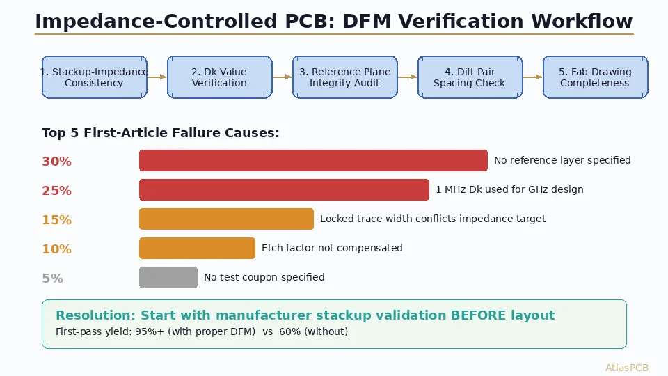
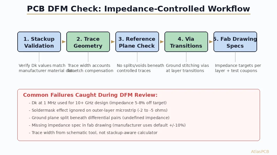
A proper PCB DFM check for impedance-controlled boards verifies five critical areas before manufacturing release: stackup layer assignment matches the impedance model, trace widths and spacing align with the target impedance within fabrication tolerances, via transitions include proper ground stitching, reference planes are continuous beneath all controlled traces, and the fab drawing specifies exact impedance targets with test coupon requirements.
Quick Answer: The 5-Point Impedance DFM Checklist
Before releasing any impedance-controlled design for manufacturing, verify:
- Stackup model uses actual manufacturer material Dk/Df values (not datasheet typical)
- Trace widths account for etch compensation (add 0.5-1.0 mil to target for inner layers)
- Reference planes are continuous — no splits, slots, or clearance voids beneath controlled traces
- Via transitions include return-path stitching vias within 2x the line spacing
- Fab drawing specifies impedance targets per layer class, tolerance, and test coupon requirements
If any of these fail, your board will either not meet impedance specs, require costly engineering hold during production, or ship with uncaught signal integrity issues.
Why Impedance-Controlled Boards Need a Different DFM Approach
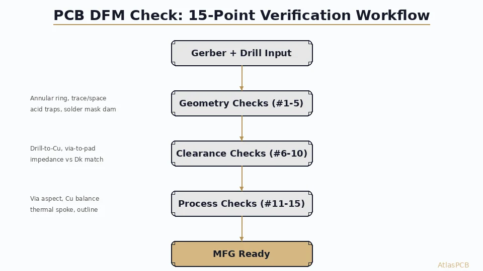
Standard DFM checks focus on manufacturability — can the factory physically produce this board without defects? Annular ring adequacy, acid trap detection, solder mask clearance, drill-to-copper spacing. These checks matter, but they tell you nothing about whether your controlled-impedance traces will actually meet their target values after fabrication.
Impedance DFM adds a layer of electrical verification on top of physical manufacturability. The trace that passes all standard DFM rules (adequate width, proper spacing from adjacent features, sufficient clearance to vias) may still produce incorrect impedance if the stackup assumptions don’t match production reality, if the trace sits over a plane split, or if etch compensation isn’t factored into the design.
In our production facility, we catch impedance-related DFM issues on approximately 25-30% of first-time customer designs. The most frequent issue — trace widths calculated using generic FR-4 Dk of 4.2 instead of the actual prepreg Dk at the target frequency, which can range from 3.8 to 4.5 depending on resin content and glass style. A Dk error of 0.3 shifts impedance by 5-8% on a typical stripline geometry, which may push the as-built board outside specified tolerance.
IMPEDANCE CONTROL EXPERTS
We Simulate Your Stackup With Our Actual Materials
Our process engineers run field-solver verification using production Dk/Df data before panel fabrication begins — catching impedance issues before they become costly respins.
Upload Design for Review ›
Step 1: Stackup Validation Against Manufacturing Reality
The stackup is where impedance control succeeds or fails. Your EDA tool’s stackup manager shows nominal dielectric thicknesses and Dk values, but these are approximations of what the factory will actually build.
The first DFM step is reconciling your design stackup with the manufacturer’s available materials. Prepreg comes in specific glass styles (1080, 2116, 7628) with specific resin contents (typically 50-68%). Each combination has a different Dk value and pressed thickness. Core materials are available in standard thicknesses. Your 4.5-mil dielectric layer might actually build at 4.2 or 4.8 mils depending on which prepreg the manufacturer assigns.
The critical information to verify:
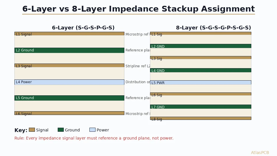
Prepreg selection: Which glass style and resin content will be used? A 2116 prepreg at 52% resin content has Dk of approximately 4.25 at 1 GHz, while a 1080 at 65% resin content measures closer to 3.9. This difference alone can shift a 50-ohm stripline by 3-4 ohms.
Core thickness tolerance: Standard cores are specified at +/-10% thickness. For impedance-critical layers, request cores with tighter thickness selection (+/-5%) or ensure your impedance calculation accounts for the worst-case thickness variation.
Copper roughness: The Dk value of the dielectric is measured on smooth copper surfaces, but production copper (especially after oxide treatment for adhesion) has surface roughness that effectively increases the electrical dielectric thickness. For designs above 5 GHz, specify the copper foil grade (standard, RTF, VLP) in your stackup.
Pressed thickness prediction: Multi-ply prepreg stacks compress differently depending on the copper pattern on adjacent layers. Areas with dense copper patterns result in thinner dielectric after pressing. Manufacturers with proper impedance capability model this copper density effect in their stackup simulation.
Step 2: Trace Geometry and Etch Compensation
The trace width you design in your CAD tool is the artwork dimension — the pattern on the phototool. The actual copper trace after etching is narrower due to the etch factor. This is well-understood in manufacturing, but designers often neglect it in their impedance calculations.
For inner layers (stripline), typical etch compensation adds 0.5-0.7 mil to each side of the trace. A trace designed at 4.0 mil artwork produces approximately 3.3-3.5 mil finished copper width on inner layers. For outer layers (microstrip), the etch factor is typically 0.7-1.0 mil per side due to the thicker copper and longer etch time.
The DFM verification workflow:
First, confirm that your impedance simulation used finished trace width (post-etch) — not artwork width. Many designers inadvertently simulate with the as-drawn width, producing an optimistic impedance estimate that the board cannot meet in production.
Second, verify that differential pair spacing is measured edge-to-edge, not center-to-center, in your impedance model. The coupling between differential traces depends on the gap distance, and that gap increases after etching even as trace width decreases.
Third, check trace width consistency along the controlled path. BGA breakout regions often have necked-down traces that deviate from the calculated impedance width. While short discontinuities (under 5mm) may be acceptable at lower frequencies, PCIe Gen5 and USB4 signaling at 16-32 GT/s is sensitive to impedance variations even over 2-3mm lengths.
Our production process maintains etch tolerance of +/-0.5 mil on finished trace width for standard processes and +/-0.3 mil for our controlled-etch workflow used on boards with +/-5% impedance tolerance. We verify this with automated optical inspection (AOI) on every panel against the target artwork dimensions.
Step 3: Reference Plane Continuity
This is the most common impedance-related DFM failure we encounter — and often the hardest for designers to identify in their own layouts because it requires visualizing the cross-sectional field distribution beneath each trace.
A controlled-impedance trace derives its impedance from the geometry between the signal conductor and its reference plane. If that reference plane has a gap, slot, or void beneath the trace, the impedance shifts upward (less capacitance to the reference) and the return current is forced to flow around the discontinuity, creating a radiating slot antenna.
Common violations we catch during DFM review:
Power plane splits beneath signal traces: Multi-voltage boards often split the power plane into islands (3.3V, 1.8V, 1.2V). Controlled-impedance traces routed across these splits see undefined impedance in the gap region. The fix is either routing around splits or adding stitching capacitors across the gap to provide a high-frequency return path.
Component clearance voids: Thermal relief connections to through-hole component pads create spoke-pattern voids in the plane. If these pads sit beneath controlled traces, the impedance is locally disturbed. This is especially problematic with legacy connectors that have irregular pad patterns on inner layers.
Via anti-pads on reference planes: Dense via fields (BGA escape arrays, decoupling cap vias) create swiss-cheese patterns in reference planes. Individual anti-pads may be acceptable if they don’t directly underlie controlled traces, but when anti-pad fields overlap with controlled trace routing, impedance becomes unpredictable.
The DFM check should include a layer-by-layer overlay verification: for each controlled-impedance net, verify that the assigned reference plane layer has continuous copper coverage for the full length of the trace routing, with anti-pad encroachment no closer than 3x the dielectric thickness.
STACKUP VERIFICATION
We Catch Reference Plane Issues Before Production
Our DFM review includes cross-sectional impedance analysis at every layer transition and plane discontinuity point along your controlled traces.
View Our DFM Process ›Step 4: Via Transitions and Return Path Stitching
Every via transition moves a signal between layers, which typically means changing the reference plane. A trace on layer 3 referenced to the ground plane on layer 2, transitioning via a through-hole to layer 6 referenced to the ground plane on layer 7, creates a discontinuity in the return current path.
The return current must find a path between layer 2 ground and layer 7 ground at the via location. Without explicit stitching vias providing this path, the return current takes a circuitous route through decoupling capacitors or distant ground via connections, creating a current loop that radiates EMI and causes impedance discontinuity at the transition point.
The DFM rule: every signal via that transitions between reference planes requires at least one ground stitching via within a radius of 2x the controlled trace spacing (for differential pairs) or 2x the dielectric thickness (for single-ended traces) from the signal via. For high-speed differential pairs above 10 Gbps, place ground stitching vias on both sides of the differential pair vias.
During our DFM review, we flag every controlled-impedance via transition that lacks adequate return-path stitching. This is one of the highest-value catches because the board will physically manufacture without the stitching vias, but signal integrity degrades significantly — particularly visible as increased insertion loss, return loss spikes at specific frequencies corresponding to the stub resonance, and elevated common-mode noise on differential pairs.
Step 5: Fabrication Drawing Specifications
The final — and surprisingly often inadequate — element of impedance DFM is the fabrication drawing itself. The drawing is your contract with the manufacturer. If impedance requirements are ambiguous, unstated, or incorrectly specified, the manufacturer has no obligation (or ability) to deliver controlled impedance.
Your fabrication drawing must specify:
Impedance table with layer-specific targets: Not “all controlled impedance traces are 50 ohms.” Specify: “Layer 3 single-ended 50 ohm +/-7%, Layer 4/5 differential 100 ohm +/-7%, Layer 7 single-ended 50 ohm +/-10%.” Different layers may have different tolerances based on their criticality.
Trace width and spacing for each impedance class: “SE50: 4.2 mil trace, reference L2 GND. DP100: 4.0/4.0 mil trace, 5.5 mil space, reference L2/L4 GND.” This tells the manufacturer exactly which traces to measure and what geometry to maintain.
Test coupon requirements: Specify whether you require TDR test coupons on every panel (standard for production), every lot (acceptable for some applications), or first-article only. Also specify whether you need individual impedance test reports shipped with the boards.
Material constraints: If your impedance calculation depends on specific material properties, specify the material by grade: “Use Isola 370HR or equivalent with Dk 3.92 +/-0.05 at 1 GHz” — not just “FR-4.”
Stackup notes: “Manufacturer to verify impedance targets are achievable with proposed stackup materials before production. Any material substitution requires re-simulation and engineer approval.”
COMPLETE DFM WORKFLOW
Impedance Verification from Stackup to TDR Report
We simulate, fabricate, and measure — delivering impedance test documentation with every controlled-impedance order. Upload your design to start the process.
Start DFM Review ›Common Mistakes That Pass Physical DFM but Fail Impedance
These issues are invisible to standard automated DFM tools but will cause impedance failures in production:
Using Dk at 1 MHz for a 10+ GHz design: FR-4 Dk drops with frequency (4.2 at 1 MHz to 3.8 at 10 GHz for typical material). If your design operates at high frequencies but your impedance model uses low-frequency Dk, the as-built impedance will be lower than target.
Ignoring soldermask thickness on outer-layer microstrip: Soldermask adds a dielectric layer on top of outer-layer traces, reducing impedance by 2-5 ohms depending on mask thickness and coverage. Specify whether your impedance target includes or excludes soldermask effect, and use a soldermask-aware impedance model for outer layers.
Differential pair breakout regions without impedance matching: BGA escape zones often neck down trace width and alter spacing to fit between pad rows. If these transitions are longer than one-tenth of the signal wavelength, they create measurable impedance discontinuities. Either maintain controlled geometry through the breakout or accept and document the deviation.
Copper balancing neglect: Panels with unbalanced copper between layers can bow and twist during lamination, locally changing dielectric thickness. For tight-tolerance impedance boards, copper balancing (thieving) on signal layers prevents this dimensional distortion from degrading impedance uniformity across the panel.
Choosing an Impedance-Controlled PCB Manufacturer: What to Ask
Not all manufacturers who claim impedance control capability deliver equivalent results. The discriminating questions:
- What field solver do they use for stackup simulation? (Polar Si9000, Simbeor, or equivalent 2D solver is minimum)
- Do they simulate with their actual production material Dk data or generic values?
- What is their standard impedance measurement protocol? (TDR on every panel, lot sampling, or first-article only?)
- Can they provide impedance test reports with individual trace measurements?
- What is their standard impedance tolerance? (+/-10% is baseline; +/-7% shows capability; +/-5% indicates advanced process control)
- Do they build test coupons into the panel, and are coupons measured on every production panel?
A manufacturer who answers these questions with specific technical detail is one who controls their impedance process. A manufacturer who responds with marketing generalities likely treats impedance as an afterthought.
ATLASPCB
Impedance-Controlled PCB Manufacturing, Done Right
Polar Si9000 simulation, TDR verification on every production panel, +/-5% tolerance available. Upload your design for manufacturer-verified stackup analysis.
Get Impedance-Controlled Quote ›
Reviewed by AtlasPCB Engineering Team — 15+ years in advanced PCB fabrication for RF, HDI, and rigid-flex applications.
Related Reading:
About AtlasPCB — We specialize in complex PCB manufacturing for HDI, RF, and high-reliability applications. Explore our impedance-controlled PCB manufacturing, free engineering DFM review, or get an full PCB manufacturing capabilities . Every order includes free engineering review. Get your quote.
Reviewed by AtlasPCB Engineering Team — IPC-certified manufacturing specialists with 15+ years of production experience in HDI, RF, and high-reliability PCB fabrication. Content based on factory floor data and real customer design reviews.
Frequently Asked Questions
What should a PCB DFM check include for impedance-controlled traces?
How does an impedance-controlled PCB manufacturer verify impedance compliance?
What impedance tolerance should I specify in my fab drawing?
What are the most common DFM errors on impedance-controlled PCBs?
Should I send my impedance stackup file to the manufacturer?
- PCB DFM check
- impedance controlled PCB manufacturer
- PCB stackup design guide
- DFM verification
- PCB manufacturing